Document number SPEC-2651AG
Specifications are subject to change without notice.
SPECIFICATION CONDITIONS
This document contains specifications and supplemental information for the Model 2651A High Power System SourceMeter™ instrument. Specifications are the standards against which the 2651A is tested. Upon leaving the factory, the 2651A meets these specifications. Supplemental and typical values are nonwarranted, apply at 23 °C, and are provided solely as useful information.
Accuracy specifications are applicable for both normal and high-capacitance modes.
Source and measurement accuracies are specified at the 2651A terminals under these conditions:
- 18 °C to 23 °C, < 70 percent relative humidity
- After two-hour warm-up
- Speed normal (1 NPLC)
- A/D autozero enabled
- Remote sense operation or properly zeroed local operation
- Calibration period: One year
DC POWER SPECIFICATIONS
| Voltage | Current | |
| Maximum output power and source/sink limits1 |
202 W maximum
|
202 W maximum
|
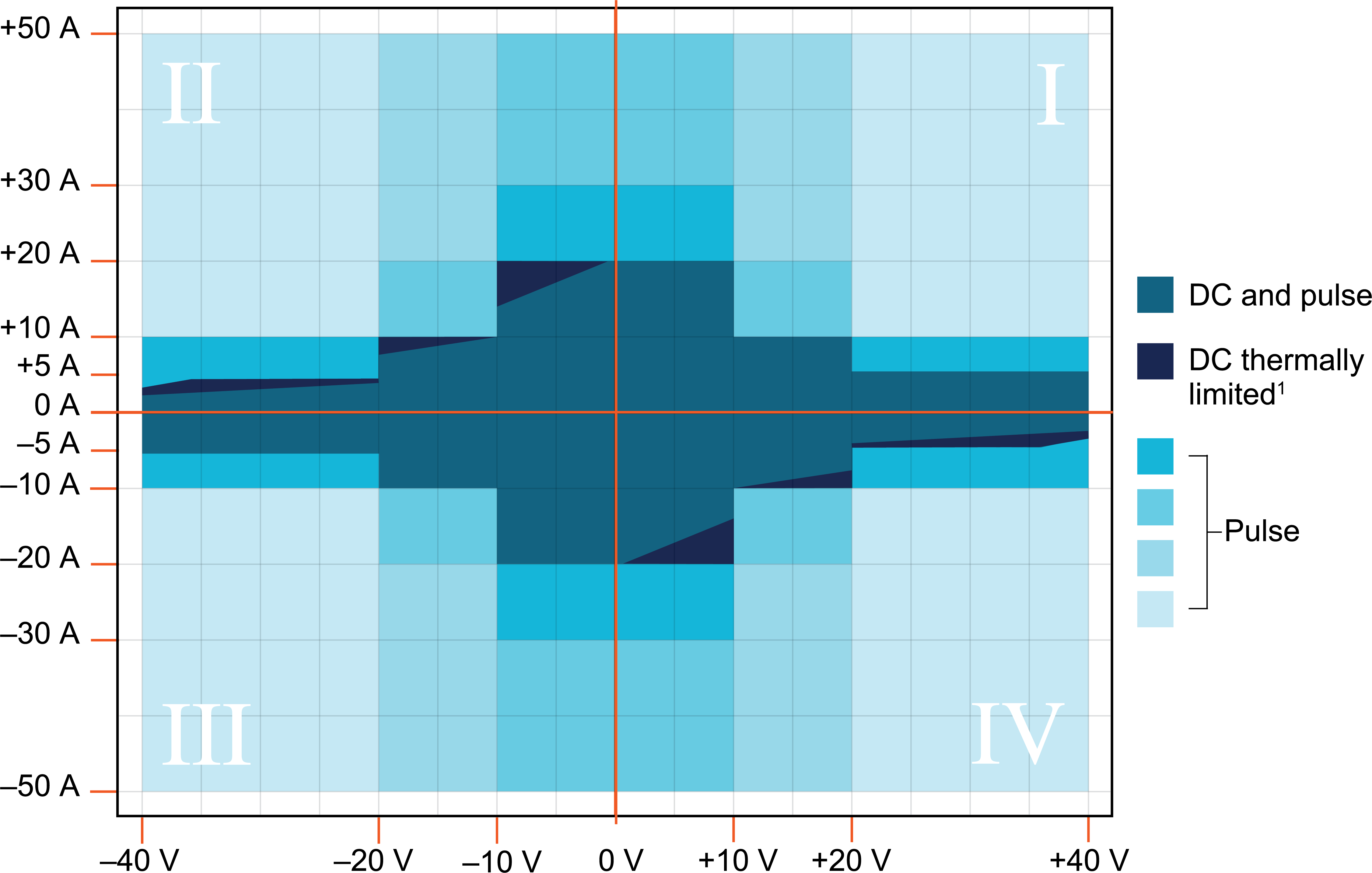
Refer to Pulse characteristics for pulsing details, such as duty cycle and pulse width.
1 Full power source operation regardless of load to 30 °C ambient. Above 30 °C or power sink operation, refer to “Operating boundaries” in the Model 2651A Reference Manual for additional power derating information and guaranteed thermal cutoffs. Typical thermal cutoffs are shown in the following table.
| Maximum output power | Voltage | Current |
| Quadrant II | –10 V at 13 A –20 V at 7.7 A –40 V at 3.3 A |
4.3 A at –20 V 10 A at –10 V 20 A at –1.3 V |
| Quadrant IV | 10 V at –13 A 20 V at –7.7 A 40 V at –3.3 A |
–4.3 A at 20 V –10 A at 10 V –20 A at 1.3 V |
2 Quadrants 2 and 4 in the power envelope are trimmed at 36 V and 4.5 A.
VOLTAGE ACCURACY SPECIFICATIONS3, 4
| Range | Source | Current | |||
| Programming resolution | Accuracy ± (% reading + volts) |
Display resolution | Integrating ADC accuracy5 ± (% reading + volts) |
High speed ADC accuracy6 ± (% reading + volts) |
|
| 100 mV | 5 µV | 0.02% + 500 µV | 100 nV | 0.02% + 300 µV | 0.05% + 600 µV |
| 1 V | 50 µV | 0.02% + 500 µV | 1 µV | 0.02% + 300 µV | 0.05% + 600 µV |
| 10 V | 500 µV | 0.02% + 5 mV | 10 µV | 0.02% + 3 mV | 0.05% + 8 mV |
| 20 V | 500 µV | 0.02% + 5 mV | 10 µV | 0.02% + 5 mV | 0.05% + 8 mV |
| 40 V | 500 µV | 0.02% + 12 mV | 10 µV | 0.02% + 12 mV | 0.05% + 15 mV |
CURRENT ACCURACY SPECIFICATIONS7
| Range | Source | Current | |||
| Programming resolution | Accuracy ± (% reading + volts) |
Display resolution | Integrating ADC accuracy5 ± (% reading + amperes) |
High speed ADC accuracy6 ± (% reading + amperes) |
|
| 100 nA | 2 pA | 0.1% + 500 pA | 100 fA | 0.08% + 500 pA | 0.08% + 800 pA |
| 1 µA | 20 pA | 0.1% + 2 nA | 1 pA | 0.08% + 2 nA | 0.08% + 4 nA |
| 10 µA | 200 pA | 0.1% +10 nA | 10 pA | 0.08% + 8 nA | 0.08% +10 nA |
| 100 µA | 2 nA | 0.03% + 60 nA | 100 pA | 0.02% + 25 nA | 0.05% + 60 nA |
| 1 mA | 20 nA | 0.03% +300 nA | 1 nA | 0.02% +200 nA | 0.05% + 500 nA |
| 10 mA | 200 nA | 0.03% + 8 µA | 10 nA | 0.02% + 2.5 µA | 0.05% + 10 µA |
| 100 mA | 2 µA | 0.03% + 30 µA | 100 nA | 0.02% + 20 µA | 0.05% + 50 µA |
| 1 A | 200 µA | 0.08% + 3.5 mA | 1 µA | 0.05% + 3 mA | 0.05% + 5 mA |
| 5 A | 200 µA | 0.08% + 3.5 mA | 1 µA | 0.05% + 3 mA | 0.05% + 5 mA |
| 10 A | 500 µA | 0.15% + 6 mA | 10 µA | 0.12% + 6 mA | 0.12% + 12 mA |
| 20 A | 500 µA | 0.15% + 8 mA | 10 µA | 0.08% + 8 mA | 0.08% + 15 mA |
| 50 A8 | 2 mA | 0.15% + 80 mA | 10 µA | 0.05% + 50 mA9 | 0.05% + 90 mA10 |
3 Add 50 µV to source accuracy specifications per volt of HI lead drop.
4 For temperatures 0 °C to 18 °C and 28 °C to 50 °C, accuracy is degraded by ± (0.15 × accuracy specification)/°C. High-capacitance mode accuracy is applicable at 23 °C ± 5 °C only.
5 Derate accuracy specification for NPLC setting < 1 by increasing error term. Add appropriate typical percent of range term for resistive loads using the table below.
| NPLC Settings | 100 mV range | 1 V to 40 V ranges | 100 nA range | 1 µA to 100 mA ranges | 1 A to 20 A ranges |
| 0.1 | 0.01% | 0.01% | 0.01% | 0.01% | 0.01% |
| 0.01 | 0.08% | 0.07% | 0.1% | 0.05% | 0.1% |
| 0.001 | 0.8% | 0.6% | 1% | 0.5% | 1.8% |
6 18-bit ADC. Average of 1000 samples taken at 100 µs intervals.
7 At temperatures 0 °C to 18 °C and 28 °C to 50 °C; 100 nA to 10 µA accuracy is degraded by ± (0.35 × accuracy specification)/°C. 100 µA to 50 A accuracy is degraded by ± (0.15 × accuracy specification)/°C. High-capacitance mode accuracy is applicable at 23 °C ± 5 °C only
8 8 50 A range accessible only in pulse mode.
9 50 A range accuracy measurements are taken at 0.008 NPLC.
10 Average of 100 samples taken at 1 µs intervals.
SUPPLEMENTAL CHARACTERISTICS
The following specifications are supplemental characteristics that provide additional information about instrument functions and performance. These characteristics are not guaranteed specifications; they describe the typical performance of the 2651A.
PULSE CHARACTERISTICS
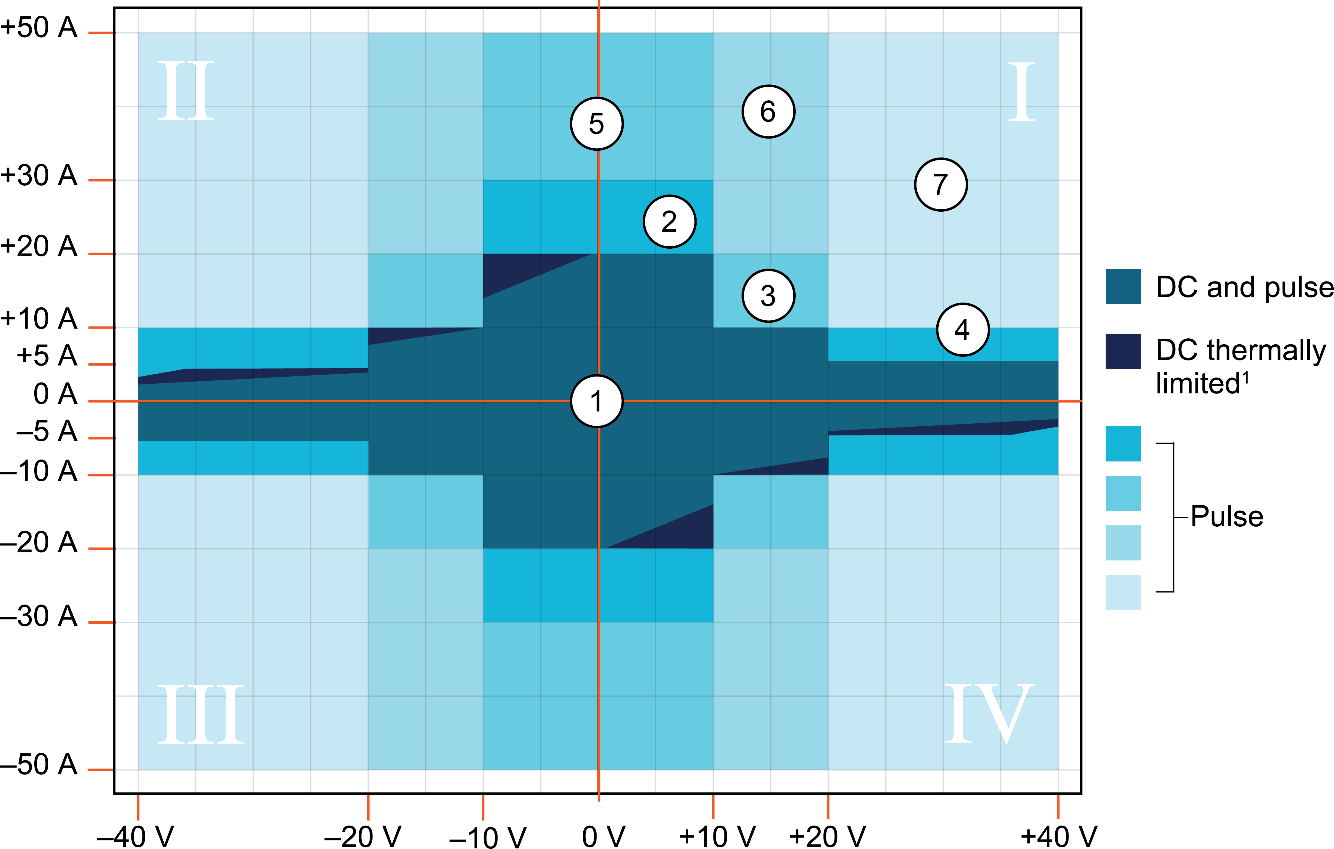
| Pulse region characteristics | Pulse region characteristics | |||
| Region | Region maximums | Maximum pulse width11 | Maximum duty cycle12 | |
| 1 | 5 A at 40 V | DC, no limit | 100% | |
| 1 | 10 A at 20 V | DC, no limit | 100% | |
| 1 | 20 A at 10 V | DC, no limit | 100% | |
| 2 | 30 A at 10 V | 1 ms | 50% | |
| 3 | 20 A at 20 V | 1.5 ms | 40% | |
| 4 | 10 A at 40 V | 1.5 ms | 40% | |
| 5 | 50 A at 10 V | 1 ms | 35% | |
| 6 | 50 A at 20 V | 330 µs | 10% | |
| 7 | 50 A at 40 V | 300 µs | 1% | |
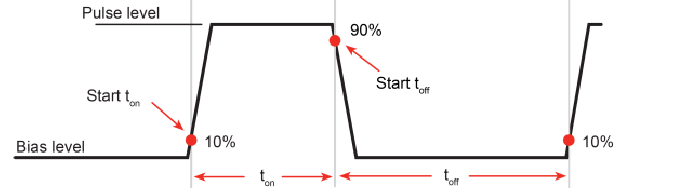
11 Times measured from the start of pulse to the start off-time; see figure below.
12 Thermally limited in sink mode (quadrants 2 and 4) and ambient temperatures above 30 °C. See power equations in the Model 2651A Reference Manual for more information.
CAUTION Carefully consider and configure the appropriate output-off state and source and compliance levels before connecting the 2651A to a device that can deliver energy. Failure to consider the output-off state and source and compliance levels may result in damage to the instrument or to the device under test.
| Current and voltage range expansion | Two 2651A instruments can be combined in series or parallel to expand the operating ranges and power performance for some applications. Refer to tek.com/keithley for the necessary application notes. | ||
| Minimum programmable pulse width13 | 100 µs Note: Minimum pulse width for settled source at a given I/V output and load can be longer than 100 µs |
||
| Pulse width programming resolution | 1 µs | ||
| Pulse width programming accuracy13 | ± 5 µs | ||
| Pulse width jitter | 2 µs | ||
| Pulse rise time | Current range | RLOAD | Rise time |
| 50 A | 0.05 Ω | 26 µs | |
| 50 A | 0.2 Ω | 57 µs | |
| 50 A | 0.4 Ω | 85 µs | |
| 20 A | 0.5 Ω | 95 µs | |
| 50 A | 0.8 Ω | 130 µs | |
| 20 A | 1 Ω | 180 µs | |
| 10 A | 2 Ω | 330 µs | |
| 5 A | 8.2 Ω | 400 µs | |
13 Times measured from the start of pulse to the start off-time; see figure below.
ADDITIONAL SOURCE CHARACTERISTICS
| Noise 10 Hz to 20 MHz |
< 100 mV peak-peak, < 30 mVRMS
|
|||
| Noise 0.1 Hz to 10 Hz |
Voltage:
Current:
|
|||
| Overshoot |
Voltage:
Current:
|
|||
| Transient response time | 10 V and 20 V ranges: < 70 µs for the output to recover to within 0.1% for a 10% to 90% step change in load 40 V range: <110 µs for the output to recover to within 0.1% for a 10% to 90% step change in load |
|||
| Range change overshoot |
Voltage:
Current:
|
|||
| Current source output settling time | Time required to reach within 0.1% of final value after source level command is processed on a fixed range Values below for IOUT × RLOAD |
|||
| Current range | RLOAD | Settling time | ||
| 20 A | 0.5 Ω | < 195 µs | ||
| 10 A | 1.5 Ω | < 540 µs | ||
| 5 A | 5 Ω | < 560 µs | ||
| 1 A | 1 Ω | < 80 µs | ||
| 100 mA | 10 Ω | < 80 µs | ||
| 10 mA | 100 Ω | < 210 µs | ||
| 1 mA | 1 kΩ | < 300 µs | ||
| 100 µA | 10 kΩ | < 500 µs | ||
| 10 µA | 100 kΩ | < 15 ms | ||
| 1 µA | 1 MΩ | < 35 ms | ||
| 100 nA | 10 MΩ | < 110 ms | ||
| Voltage source output settling time | Time required to reach within 0.1% of final value after source level command is processed on a fixed range14 | |||
| Range | Settling time | |||
| 1 V | < 70 µs | |||
| 10 V | < 160 µs | |||
| 20 V | < 190 µs | |||
| 40 V | < 175 µs | |||
| Guard offset voltage |
< 4 mV
|
|||
| Remote sense operating range15 | Maximum voltage between HI and SENSE HI = 3 V Maximum voltage between LO and SENSE LO = 3 V |
|||
| Maximum impedance per source lead |
Maximum impedance limited by 3 V drop by remote sense operating range
|
|||
| Voltage output headroom |
5 A range
10 A range
20 A range
|
|||
| Overtemperature protection | Internally sensed temperature overload puts unit in standby mode | |||
| Limit/compliance |
Bipolar limit (compliance) set with single value
Current:17
|
|||
ADDITIONAL METER CHARACTERISTICS
| Contact check characteristics18 | Speed | Maximum measurement time to memory for 60 Hz (50 Hz) | Accuracy (1 year) 23 °C ± 5 °C ± (% reading + ohms) |
| Fast | 1.1 ms (1.2 ms) | 5% + 15 Ω | |
| Medium | 4.1 ms (5 ms) | 5% + 5 Ω | |
| Slow | 36 ms (42 ms) | 5% + 3 Ω |
14 With measure and compliance set to the maximum current for the specified voltage range.
15 Add 50 µV to source accuracy specifications per volt of HI lead drop.
16 For sink mode operation (quadrants II and IV), add 0.6 percent of limit range to the corresponding voltage source accuracy specifications. For 100 mV range add an additional 60 mV of uncertainty. Specifications apply with sink mode enabled.
17 For sink mode operation (quadrants II and IV), add 0.6 percent of limit range to the corresponding current limit accuracy specifications. Specifications apply with sink mode enabled.
18 Includes measurement of SENSE HI to HI and SENSE LO to LO contact resistances.
| Maximum load impedance | Normal mode 10 nF 3 µH |
High capacitance mode 50 µF 3 µH |
| Common mode voltage | 250 V dc | |
| Common mode isolation | > 1 GΩ < 4500 pF |
|
| Measure input impedance | > 10 GΩ | |
| Sense high input impedance | > 10 GΩ | |
| Maximum sense lead resistance | 1 kΩ for rated accuracy | |
| Overrange | 101% of source range 102% of measure range |
|
HIGH-CAPACITANCE MODE CHARACTERISTICS 19, 20
| Accuracy characteristics21 | Accuracy characteristics are applicable in both normal and high capacitance modes | |
| Voltage source output settling time | Time required to reach within 0.1% of final value after source level command is processed on a fixed range22 | |
| Voltage source range | Settling time with CLOAD = 4.7 µF | |
| 1 V | 75 µs | |
| 10 V | 170 µs | |
| 20 V | 200 µs | |
| 40 V | 180 µs | |
| Mode change delay |
Current ranges of 100 µA and above:
Current ranges below 100 µA:
|
|
| Measure input impedance | > 10 GΩ in parallel with 25 nF | |
| Voltage source range change overshoot |
< 400 mV + 0.1% of larger range
|
|
19 High-capacitance mode specifications are for dc measurements only and use locked ranges. Autorange is disabled.
20 100 nA range is not available in high-capacitance mode.
21 Add an additional 2 nA to the source current accuracy and measure current accuracy offset for the 1 µA range.
22 With measure and compliance set to the maximum current for the specified voltage range.
MEASUREMENT SPEED CHARACTERISTICS23, 24
Maximum sweep operation rates (operations per second) for 60 Hz (50 Hz):
| A/D converter speed | Trigger origin | Measure to memory using user scripts |
Measure to GPIB using user scripts |
Source measure to memory using user scripts |
Source measure to GPIB using user scripts |
Source measure to memory using sweep API |
Source measure to GPIB using sweep API |
| 0.001 NPLC | Internal | 20000 (20000) |
9800 (9800) |
7000 (7000) |
6200 (6200) |
12000 (12000) |
5900 (5900) |
| 0.001 NPLC | Digital I/O | 8100 (8100) |
7100 (7100) |
5500 (5500) |
5100 (5100) |
11200 (11200) |
5700 (5700) |
| 0.01 NPLC | Internal | 4900 (4000) |
3900 (3400) |
3400 (3000) |
3200 (2900) |
4200 (3700) |
4000 (3500) |
| 0.01 NPLC | Digital I/O | 3500 (3100) |
3400 (3000) |
3000 (2700) |
2900 (2600) |
4150 (3650) |
3800 (3400) |
| 0.1 NPLC | Internal | 580 (480) |
560 (470) |
550 (465) |
550 (460) |
560 (470) |
545 (460) |
| 0.1 NPLC | Digital I/O | 550 (460) |
550 (460) |
540 (450) |
540 (450) |
560 (470) |
545 (460) |
| 1.0 NPLC | Internal | 59 (49) |
59 (49) |
59 (49) |
59 (49) |
59 (49) |
59 (49) |
| 1.0 NPLC | Digital I/O | 58 (48) |
58 (49) |
59 (49) |
59 (49) |
59 (49) |
59 (49) |
| High-speed ADC |
Internal | 38500 (38500) |
18000 (18000) |
10000 (10000) |
9500 (9500) |
14300 (14300) |
6300 (6300) |
| High-speed ADC |
Digital I/O | 12500 (12500) |
11500 (11500) |
7500 (7500) |
7000 (7000) |
13200 (13200) |
6000 (6000) |
High-speed ADC burst measurement rates:25
| Burst length (readings) | Readings per second | Bursts per second |
| 100 | 1,000,000 | 400 |
| 500 | 1,000,000 | 80 |
| 1000 | 1,000,000 | 40 |
| 2500 | 1,000,000 | 16 |
| 5000 | 1,000,000 | 8 |
23 Tests performed with a 2651A on channel A using the following equipment: Computer hardware (Intel® Pentium® 4 2.4 GHz, 2 GB RAM, National Instruments™ PCI-GPIB); driver (NI-488.2 Version 2.2 PCI-GPIB); software (Microsoft® Windows® XP, Microsoft® Visual Studio® 2010, NI-VISA™ version 4.1).
24 Exclude current measurement ranges less than 1 mA.
25 smua.measure.adc must be enabled and the smua.measure.count set to the burst length.
Maximum single measurement rates (operations per second) for 60 Hz (50 Hz):
| A/D converter speed | Trigger origin | Measure to GPIB | Source measure to GPIB | Source measure pass/fail to GPIB |
| 0.001 NPLC | Internal | 1900 (1800) | 1400 (1400) | 1400 (1400) |
| 0.01 NPLC | Internal | 1450 (1400) | 1200 (1100) | 1100 (1100) |
| 0.1 NPLC | Internal | 450 (390) | 425 (370) | 425 (375) |
| 1.0 NPLC | Internal | 58 (48) | 57 (48) | 57 (48) |
| Maximum measurement range change rate | > 4000 per second for > 10 µA |
| Maximum source range change rate | 10 ms for ranges > 100 μA and < 5 A 30 ms for ranges ≥ 5 A |
| Command processing time | Maximum time required for the output to begin to change following the receipt of the smua.source.levelv or smua.source.leveli command; < 1 ms |
TRIGGERING AND SYNCHRONIZATION CHARACTERISTICS
Triggering
| Trigger in to trigger out | 0.5 μs |
| Trigger in to source change26 | 10 μs |
| Trigger timer accuracy | ± 2 μs |
| Source change26 after LXI trigger | 280 μs |
Synchronization
| Single-node synchronized source change26 | < 0.5 μs |
| Multi-node synchronized source change26 | < 0.5 μs |
26 Fixed source range with no polarity change.
SUPPLEMENTAL INFORMATION
| Front-panel interface | Two-line vacuum fluorescent display (VFD) with keypad and navigation wheel |
| Display |
|
| Keypad operations |
|
| Programming | Embedded Test Script Processor (TSP™) accessible from any host interface; responds to high-speed test scripts comprised of remote commands and statements (for example, branching, looping, and math); able to execute test scripts stored in memory without host intervention |
| Minimum user memory available | 16 MB (approximately 250,000 lines of TSP code) |
| Reading buffers |
Nonvolatile memory uses dedicated storage areas reserved for measurement data; reading buffers are arrays of measurement elements; each element can hold the following items:
Two reading buffers are reserved for each 2651A channel; reading buffers can be filled using the front-panel STORE key and retrieved using the RECALL key or host interface |
| Buffer size, with timestamp and source setting | > 60,000 samples |
| Buffer size, without timestamp and source setting | > 140,000 samples |
Timing
| Timer | Free-running 47-bit counter with 1 MHz clock input; reset each time instrument power is turned on; if the instrument is not turned off, the timer is reset to zero (0) every four years |
| Timestamp | TIMER value is automatically saved when each measurement is triggered |
| Resolution | 1 μs |
| Timestamp accuracy | ± 100 ppm |
GENERAL SPECIFICATIONS
| IEEE-488 | IEEE Std 488.1 compliant. Supports IEEE Std 488.2 common commands and status model topology | |
| RS-232 |
|
|
| Ethernet | RJ-45 connector, LXI Class C, 10/100BT, Auto MDIX | |
| LXI compliance | LXI version 1.4 Core 2011 | |
| Expansion interface |
|
|
| USB File System | USB 2.0 Host: Mass storage class device | |
| Power supply | 100 V ac to 240 V ac, 50 Hz to 60 Hz (autosensing), 550 VA maximum | |
| Cooling | Forced air; side and top intake and rear exhaust | |
| Warranty | 1 year | |
| EMC | Conforms to European Union EMC Directive | |
| Safety | UL listed to UL61010-1:2004 Conforms to European Union Low Voltage Directive |
|
| Environment | For indoor use only Altitude: Maximum 2000 m (6562 ft) above sea level Operating: 0 °C to 50 °C, 70% relative humidity up to 35 °C; derate 3% relative humidity/°C, 35 °C to 50 °C Storage: −25 °C to 65 °C |
|
| Dimensions | Rack mount: 89 mm high × 435 mm wide × 549 mm deep (3.5 in. × 17.1 in. × 21.6 in.) Bench configuration (with handle and feet): 104 mm high × 483 mm wide × 620 mm deep (4.1 in. × 19 in. × 24.4 in.) |
|
| Weight | 10.2 kg (22.5 lb) | |
| Digital I/O interface |
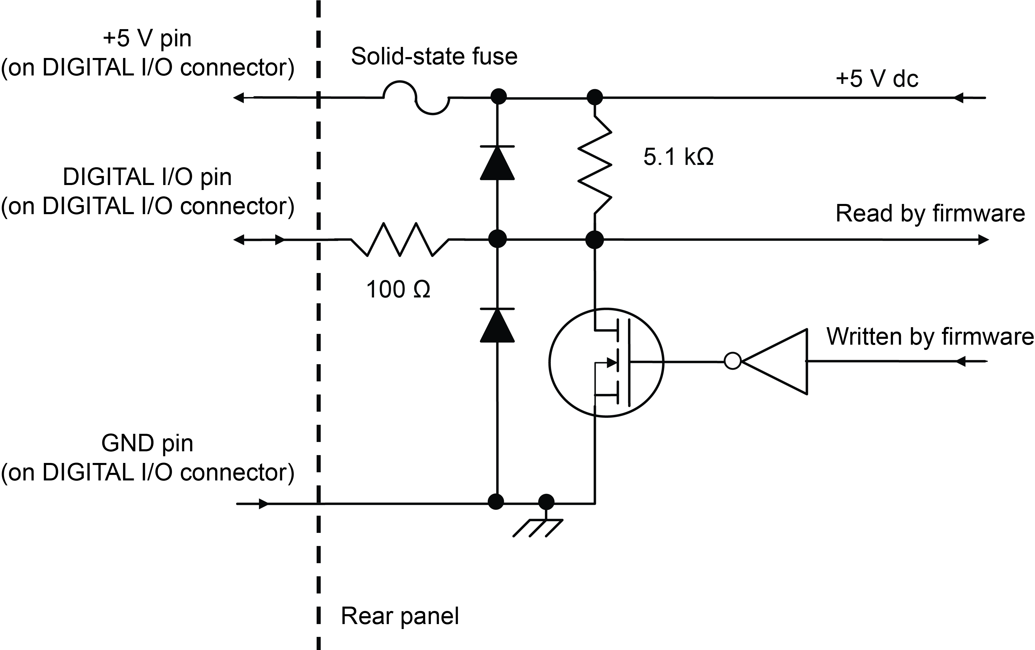
Input/output pins: 14 open drain I/O bits Absolute maximum input voltage: 5.25 V Absolute minimum input voltage: –0.25 V Maximum logic low input voltage: 0.7 V, +850 µA maximum Minimum logic high input voltage: 2.1 V, +570 µA Maximum source current (flowing out of digital I/O bit): +960 µA Maximum sink current at maximum logic low voltage (0.7 ): –5.0 mA Absolute maximum sink current (flowing into digital I/O pin): –11 mA 5 V power supply pin: Limited to 250 mA, solid-state fuse protected Output enable pin: Active high input pulled down internally to ground with a 10 kΩ resistor; when the output enable input function has been activated, the 2651A channel will not turn on unless the output enable pin is driven to > 2.1 V (nominal current = 2.1 V/10 kΩ = 210 µA) |
Find more valuable resources at TEK.COM
Copyright © Tektronix. All rights reserved. Tektronix products are covered by U.S. and foreign patents, issued and pending. Information in this publication supersedes that in all previously published material. Specification and price change privileges reserved. TEKTRONIX and TEK are registered trademarks of Tektronix, Inc. All other trade names referenced are the service marks, trademarks or registered trademarks of their respective companies.
SPEC-2651A April 2022