C-V Characterization of MOS Capacitors Using the Model 4200-SCS Parameter Analyzer
Introduction
Maintaining the quality and reliability of gate oxides of MOS structures is a critical task in a semiconductor fab. Capacitance-evoltage (C-V) measurements are commonly used in studying gate-oxide quality in detail. These measurements are made on a two-terminal device called a MOS capacitor (MOS cap), which is basically a MOSFET without a source and drain. C-V test results offer a wealth of device and process information, including bulk and interface charges. Many MOS device parameters, such as oxide thickness, flatband voltage, threshold voltage, etc., can also be extracted from the C-V data.
Using a tool such as the Keithley Model 4200-SCS equipped with the 4200-CVU Integrated C-V Option for making C-V measurements on MOS capacitors can simplify testing and analysis. The Model 4200-SCS is an integrated measurement system that can include instruments for both I-V and C-V measurements, as well as software, graphics, and mathematical analysis capabilities. The software incorporates C-V tests, which include a variety of complex formulas for extracting common C-V parameters.
This application note discusses how to use a Keithley Model 4200-SCS Parameter Analyzer equipped with the Model 4200-CVU Integrated C-V Option to make C-V measurements on MOS capacitors. It also addresses the basic principles of MOS caps, performing C-V measurements on MOS capacitors, extracting common C-V parameters, and measurement techniques. The Keithley Test Environment Interactive (KTEI) software that controls the Model 4200-SCS incorporates a list of a dozen test projects specific to C-V testing. Each project is paired with the formulae necessary to extract common C-V parameters, such as oxide capacitance, oxide thickness, doping density, depletion depth, Debye length, flatband capacitance, flatband voltage, bulk potential, threshold voltage, metal-semiconductor work function difference, and effective oxide charge. This completeness is in sharp contrast to other commercially available C-V solutions, which typically require the user to research and enter the correct formula for each parameter manually.
Overview of C-V Measurement Technique
By definition, capacitance is the change in charge (Q) in a device that occurs when it also has a change in voltage (V):
| C ≡ | ∆Q |
| ∆V |
One general practical way to implement this is to apply a small AC voltage signal (millivolt range) to the device under test, and then measure the resulting current. Integrate the current over time to derive Q and then calculate C from Q and V.
C-V measurements in a semiconductor device are made using two simultaneous voltage sources: an applied AC voltage signal (dVac) and a DC voltage (Vdc) that is swept in time, as illustrated in Figure 1.
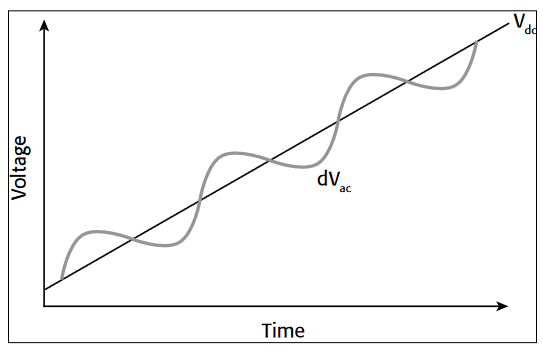
The magnitude and frequency of the AC voltage are fixed; the magnitude of the DC voltage is swept in time. The purpose of the DC voltage bias is to allow sampling of the material at different depths in the device. The AC voltage bias provides the small-signal bias so the capacitance measurement can be performed at a given depth in the device.
Basic Principles of MOS Capacitors
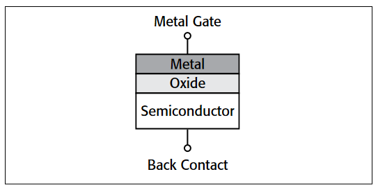
Figure 2 illustrates the construction of a MOS capacitor. Essentially, the MOS capacitor is just an oxide placed between a semiconductor and a metal gate. The semiconductor and the metal gate are the two plates of the capacitor. The oxide functions as the dielectric. The area of the metal gate defines the area of the capacitor.
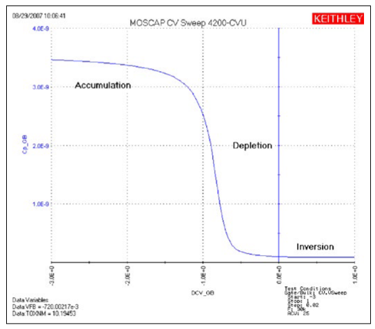
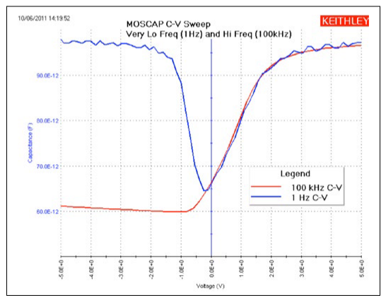
The most important property of the MOS capacitor is that its capacitance changes with an applied DC voltage. As a result, the modes of operation of the MOS capacitor change as a function of the applied voltage. Figure 3 illustrates a high frequency C-V curve for a p-type semiconductor substrate. As a DC sweep voltage is applied to the gate, it causes the device to pass through accumulation, depletion, and inversion regions.
The three modes of operation, accumulation, depletion and inversion, will now be discussed for the case of a p-type semiconductor, then briefly discussed for an n-type semiconductor at the end of this section.
Accumulation Region
With no voltage applied, a p-type semiconductor has holes, or majority carriers, in the valence band. When a negative voltage is applied between the metal gate and the semiconductor, more holes will appear in the valence band at the oxide-semiconductor interface. This is because the negative charge of the metal causes an equal net positive charge to accumulate at the interface between the semiconductor and the oxide. This state of the p-type semiconductor is called accumulation.
For a p-type MOS capacitor, the oxide capacitance is measured in the strong accumulation region. This is where the voltage is negative enough that the capacitance is essentially constant and the C-V curve is almost flat. This is where the oxide thickness can also be extracted from the oxide capacitance.
However, for a very thin oxide, the slope of the C-V curve doesn't flatten in accumulation and the measured oxide capacitance differs from the actual oxide capacitance.
Depletion Region
When a positive voltage is applied between the gate and the semiconductor, the majority carriers are replaced from the semiconductor-oxide interface. This state of the semiconductor is called depletion because the surface of the semiconductor is depleted of majority carriers. This area of the semiconductor acts as a dielectric because it can no longer contain or conduct charge. In effect, it becomes an insulator.
The total measured capacitance now becomes the oxide capacitance and the depletion layer capacitance in series, and as a result, the measured capacitance decreases. This decrease in capacitance is illustrated in Figure 3 in the depletion region. As a gate voltage increases, the depletion region moves away from the gate, increasing the effective thickness of the dielectric between the gate and the substrate, thereby reducing the capacitance.
Inversion Region
As the gate voltage of a p-type MOS-C increases beyond the threshold voltage, dynamic carrier generation and recombination move toward net carrier generation. The positive gate voltage generates electron-hole pairs and attracts electrons (the minority carriers) toward the gate. Again, because the oxide is a good insulator, these minority carriers accumulate at the substrate-to-oxide/well-to-oxide interface. The accumulated minority-carrier layer is called the inversion layer because the carrier polarity is inverted. Above a certain positive gate voltage, most available minority carriers are in the inversion layer, and further gate voltage increases do not further deplete the semiconductor. That is, the depletion region reaches a maximum depth.
Once the depletion region reaches a maximum depth, the capacitance that is measured by the high frequency capacitance meter is the oxide capacitance in series with the maximum depletion capacitance. This capacitance is often referred to as minimum capacitance. The C-V curve slope is almost flat.
NOTE: The measured inversion-region capacitance at the maximum depletion depth depends on the measurement frequency. Therefore, C-V curves measured at different frequencies may have different appearances. Generally, such differences are more significant at lower frequencies and less significant at higher frequencies.
n-type Substrate
The C-V curve for an n-type MOS capacitor is analogous to a p-type curve, except that (1) the majority carriers are electrons instead of holes; (2) the n-type C-V curve is essentially a mirror image of the p-type curve; (3) accumulation occurs by applying a positive voltage to the gate; and (4) the inversion region occurs at negative voltage.
Performing C-V Measurements with the 4200-CVU
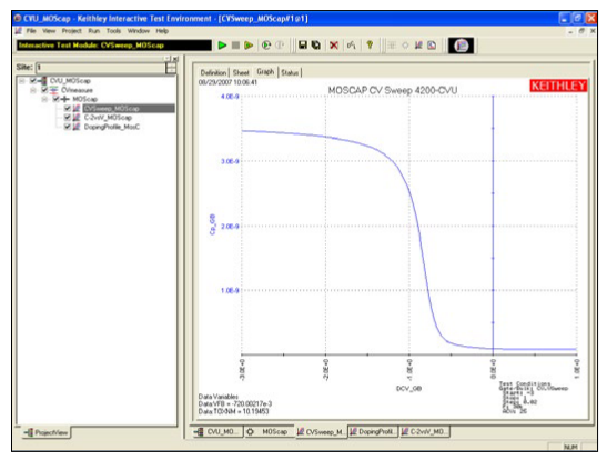
To simplify testing, a project has been created for the 4200-SCS that makes C-V measurements on a MOS capacitor and extracts common measurement parameters such as oxide thickness, flatband voltage, threshold voltage, etc. The project (CVU_MOScap) is included with all 4200-SCS systems running KTEI Version 7.0 or later. Figure 4 is a screen shot of the project, which has three tests, called ITMs (Interactive Test Modules), which generate a C-V sweep (CVSweep_MOScap), a 1/C2 vs.Gate Voltage curve (C-2vsV_MOScap), and a doping profile (DopingProfile_MosC). Figure 4 also illustrates a C-V sweep generated with the (CVSweep_MOScap) test module. All of the extracted C-V parameters in these test modules are defined in the next section of this application note.
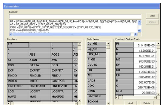
CVSweep_MOScap Test Module
This test performs a capacitance measurement at each step of a user-configured linear voltage sweep. A C-V graph is generated from the acquired data, and several device parameters are calculated using the Formulator, which is a tool in the 4200-SCS's software that provides a variety of computational functions, common mathematical operators, and common constants. Figure 5 shows the window of the Formulator. These derived parameters are listed in the Sheet Tab of the Test Module.
C-2vsV_MOScap Test Module
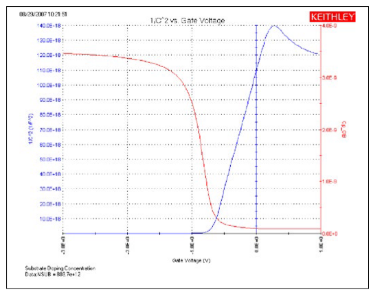
This test performs a C-V sweep and displays the capacitance (1/C2) as a function of the gate voltage (VG). This sweep can yield important information about doping profile because the substrate doping concentration (NSUB) is inversely related to the reciprocal of the slope of the 1/C2 vs. VG curve. A positive slope indicates acceptors and a negative slope indicates donors. The substrate doping concentration is extracted from the slope of the 1/C2 curve and is displayed on the graph. Figure 6 shows the results of executing this test module.
Doping Profile Test Module
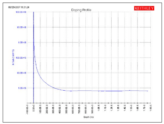
This test performs a doping profile, which is a plot of the doping concentration vs. depletion depth. The difference in capacitance at each step of the gate voltage is proportional to the doping concentration. The depletion depth is computed from the high frequency capacitance and oxide capacitance at each measured value of the gate voltage. The results are plotted on the graph as shown in Figure 7.
Connections to the 4200-CVU
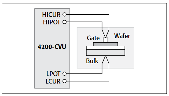
To make a C-V measurement, a MOS cap is connected to the 4200-CVU as shown in Figure 8. In the ITM, both the 4200-CVU ammeter and the DC voltage appear at the HCUR/HPOT terminals. See the next section, "Measurement Optimization," for further information on connecting the CVU to the device on a wafer.
Measurement Optimization
Successful measurements require compensating for stray capacitance, measuring at equilibrium conditions, and compensating for series resistance.
Offset Correction for Stray Capacitance
C-V measurements on a MOS capacitor are typically performed on a wafer using a prober. The 4200-CVU is designed to be connected to the prober via interconnect cables and adaptors and may possibly be routed through a switch matrix. This cabling and switch matrix will add stray capacitance to the measurements.
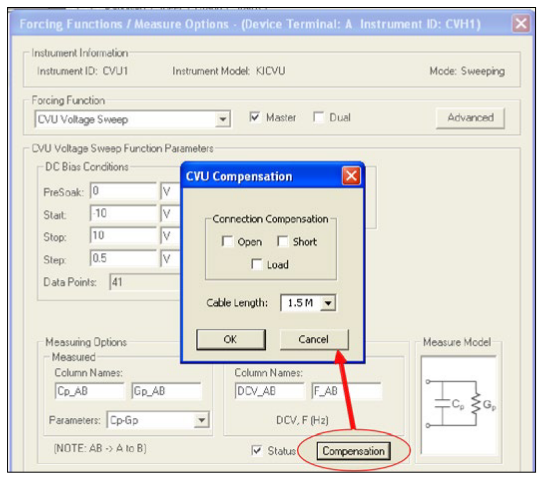
To correct for stray capacitance, the KTEI software environment has a built-in tool for offset correction, which is a two-part process: the corrections for OPEN and/or SHORT are performed first, and then they can be enabled within an ITM. To perform the corrections, Open the Tools Menu and select CVU Connection Compensation. For an Open correction, click on Measure Open. Probes must be up during the correction. Open is typically used for high impedance measurements (<10pF or >1MΩ).
For a Short correction, click on Measure Short. Short the probe to the chuck. A short correction is generally performed for low impedance measurements (>10nF or <10Ω).
After the corrections are performed, they must be enabled in the project. To enable corrections, click the Compensation button at the bottom of the Forcing Functions/Measure Options Window. In the CVU Compensation dialog box (Figure 9), click only the corrections to be applied.
Measuring at Equilibrium Conditions
A MOS capacitor takes time to become fully charged after a voltage step is applied. C-V measurement data should only be recorded after the device is fully charged. This condition is called the equilibrium condition. Therefore, to allow the MOS capacitor to reach equilibrium: (1) allow a sufficient Hold Time in the Timing Menu to enable the MOS capacitor to charge up while applying a "PreSoak" voltage, and (2) allow a sufficient Sweep Delay Time in the Timing Menu before recording the capacitance after each voltage step of a voltage sweep. The appropriate Hold and Delay Times are determined experimentally by generating capacitance vs. time plots and observing the time for the capacitance to settle.
Although C-V curves swept from different directions may look different, allowing adequate Hold and Delay Times minimizes such differences. One way to determine sufficient Hold and Delay Times is to generate a series of C-V curves in both directions. Change the Hold and Delay Times for each pair of inversion ➞ accumulation and accumulation ➞ inversion curves until the curves look essentially the same for both sweep directions.
Hold and Delay Times When Sweeping from Inversion ➞ Accumulation. When the C-V sweep starts in the inversion region and the starting voltage is initially applied, a MOS capacitor is driven into deep depletion. Thereafter, if the starting voltage is maintained, the initial high frequency C-V curve climbs toward and ultimately stabilizes to the minimum capacitance at equilibrium. However, if the initial Hold Time is too short, the MOS capacitor cannot adequately recover from deep depletion, and the measured capacitance will be smaller than the minimum capacitance at equilibrium. Set the "PreSoak" voltage to the first voltage in the voltage sweep and allow a sufficient Hold Time for the MOS capacitor to reach equilibrium.
However, once the MOS capacitor has reached equilibrium after applying the "PreSoak" voltage, an inversion ➞ accumulation C-V sweep may be performed with small delay times. This is possible because minority carriers recombine relatively quickly as the gate voltage is reduced. Nonetheless, if the Delay Time is too short, non-equilibrium occurs, and the capacitance in the inversion region is slightly higher than the equilibrium value. This is illustrated by the upper dotted line in Figure 10.
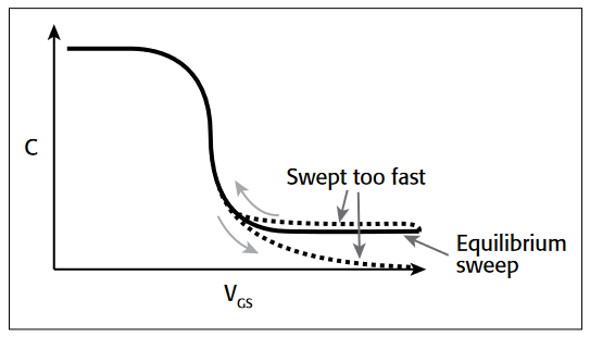
Hold and Delay Times When Sweeping from Accumulation ➞ Inversion. When the C-V sweep starts in the accumulation region, the effects of Hold and Delay Times in the accumulation and depletion regions are fairly subtle. However, in the inversion region, if the Delay Time is too small (i.e., the sweep time is too fast), there's not enough time for the MOS capacitor to generate minority carriers to form an inversion layer. On the high frequency C-V curve, the MOS capacitor never achieves equilibrium and eventually becomes deeply depleted. The measured capacitance values fall well below the equilibrium minimum value. The lower dotted line in Figure 10 illustrates this phenomenon.
Using the preferred sequence. Generating a C-V curve by sweeping from inversion to accumulation is faster and more controllable than sweeping from accumulation to inversion. Figure 11 illustrates a preferred measurement sequence.
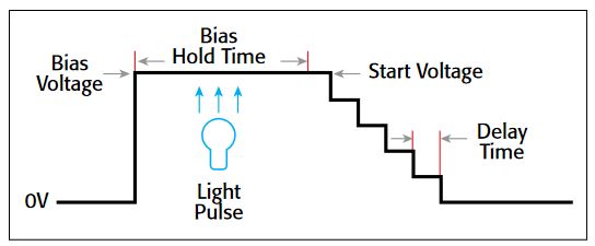
The device is first biased at the "PreSoak" voltage for the Hold Time that is adjusted in the Timing Menu. The bias or "PreSoak" voltage should be the same as the sweep start voltage to avoid a sudden voltage change when the sweep starts. During biasing, if necessary, a short light pulse can be applied to the sample to help generate minority carriers. However, before the sweep starts, all lights should be turned off. All measurements should be performed in total darkness because the semiconductor material may be light sensitive. During the sweep, the Delay Time should be chosen to create the optimal balance between measurement speed and measurement integrity, which requires adequate equilibration time.
Compensating for series resistance
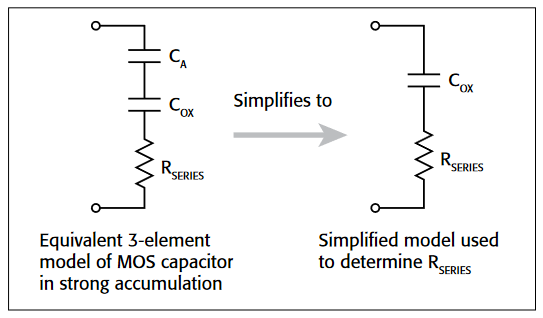
After generating a C-V curve, it may be necessary to compensate for series resistance in measurements. The series resistance (RSERIES) can be attributed to either the substrate (well) or the backside of the wafer. For wafers typically produced in fabs, the substrate bulk resistance is fairly small (<10Ω) and has negligible impact on C-V measurements. However, if the backside of the wafer is used as an electrical contact, the series resistance due to oxides can significantly distort a measured C-V curve. Without series compensation, the measured capacitance can be lower than the expected capacitance, and C-V curves can be distorted. Tests for this project compensate for series resistance using the simplified three-element model shown in Figure 12. In this model, COX is the oxide capacitance and CA is the capacitance of the accumulation layer. The series resistance is represented by RSERIES.
The corrected capacitance (CADJ) and corrected conductance (GADJ) are calculated from the following formulas [1]:
| CADJ = | (G2 + (2πƒ∁)2)∁ |
| a2R + (2πƒ∁)2 |
| GADJ = | (G2 + (2πƒ∁)2)aR |
| a2R + (2πƒ∁)2 |
where:
| aR = | G - (G2 + (2πƒ∁)2)Rs |
CADJ = series resistance compensated parallel model capacitance
C = measured parallel model capacitance
GADJ = series resistance compensated conductance
G = measured conductance
f = test frequency as set in the KITE Definition Tab
RS = series resistance
The series resistance (RS) may be calculated from the capacitance and conductance values that are measured while biasing the DUT (device under test) in the accumulation region as follows:
| RS = | (G2 + (2πƒ∁)2)aR |
| a2R + (2πƒ∁)2 |
where:
RS = series resistance
G = measured conductance
C = measured parallel model capacitance (in strong accumulation)
ƒ = test frequency as set in KITE (Definition tab)
NOTE: The preceding equations for compensating for series resistance require that the Model 4200-CVU be using the parallel model (Cp-Gp).
For this project, these formulas have been added into the KITE Formulator so the capacitance and conductance can be automatically compensated for the series resistance.
Extracting MOS Device Parameters From C-V Measurements
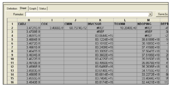
This section describes the device parameters that are extracted from the C-V data taken in the three test modules in the CVU_MOScap project. The parameters are derived in the Formulator and the calculated values appear in the Sheet tab of each test module as shown in Figure 13.
Oxide thickness
For a relatively thick oxide (>50Å), extracting the oxide thickness is fairly simple. The oxide capacitance (COX) is the high frequency capacitance when the device is biased for strong accumulation. In the strong accumulation region, the MOS-C acts like a parallel-plate capacitor, and the oxide thickness (TOX) may be calculated from COX and the gate area using the following equation:
| TOX(nm) = | (107)Aeox |
| Cox |
where:
TOX = oxide thickness (nm)
A = gate area (cm2)
eOX = permittivity of the oxide material (F/cm)
COX = oxide capacitance (F)
107 = units conversion from cm to nm
Flatband capacitance and flatband voltage
Application of a certain gate voltage, the flatband voltage (VFB), results in the disappearance of band bending. At this point, known as the flatband condition, the semiconductor band is said to become flat. Because the band is flat, the surface potential is zero (with the reference potential being taken as the bulk potential deep in the semiconductor). Flatband voltage and its shift are widely used to extract other device parameters, such as oxide charges.
VFB can be identified from the C-V curve. One way is to use the flatband capacitance method. For this method, the ideal value of the flatband capacitance (CFB) is calculated from the oxide capacitance and the Debye length. The concept of Debye length is introduced later in this section. Once the value of CFB is known, the value of VFB can be obtained from the C-V curve data, by interpolating between the closest gate-to-substrate (VGS) values [2].
The Debye length parameter (λ) must also be calculated to derive the flatband voltage and capacitance. Based on the doping profile, the λ calculation requires one of the following doping concentrations: N at 90% of WMAX (refer to Nicollian and Brews), a user-supplied NA (bulk doping concentration for a p-type, acceptor, material), or a user-supplied ND (bulk doping concentration for an n-type, donor, material).
NOTE: The flatband capacitance method is invalid when the interface trap density (DIT) becomes very large (1012–1013 or greater). However, the method should give satisfactory results for most users. When dealing with high DIT values, consult the appropriate literature for a more suitable method.
The flatband capacitance is calculated as follows:
| CFB = | Cox (εSA/λ) (102) |
| Cox + (εSA/λ) (102) |
where:
CFB = flatband capacitance (F)
COX = oxide capacitance (F)
εS = permittivity of the substrate material (F/cm)
A = gate area (cm2)
102 = units conversion from m to cm
λ = extrinsic Debye length, which is calculated as follows:
| λ = | ( | εSkT | )1/2 | (10-2) |
| q2N |
where:
λ = extrinsic Debye length
εS = permittivity of the substrate material (F/cm)
kT = thermal energy at room temperature (293K) (4.046 × 10⁻²¹J)
q = electron charge (1.60219 × 10⁻¹⁹C)
NX = N at 90% WMAX or N90W (refer to Nicollian and Brews; see References) or, when input by the user, NX = NA or NX = ND
10-2 = units conversion from cm to m
The extrinsic Debye length is an idea borrowed from plasma physics. In semiconductors, majority carriers can move freely. The motion is similar to a plasma. Any electrical interaction has a limited range. The Debye length is used to represent this interaction range. Essentially, the Debye length indicates how far an electrical event can be sensed within a semiconductor.
Threshold voltage
The turn-on region for a MOSFET corresponds to the inversion region on its C-V plot. When a MOSFET is turned on, the channel formed corresponds to strong generation of inversion charges. It is these inversion charges that conduct current. When a source and drain are added to a MOS-C to form a MOSFET, a p-type MOS-C becomes an n-type MOSFET, also called an n-channel MOSFET. Conversely, an n-type MOS-C becomes a p-channel MOSFET.
The threshold voltage (VTH) is the point on the C-V curve where the surface potential (φS) equals twice the bulk potential (φB). This curve point corresponds to the onset of strong inversion. For an enhancement-mode MOSFET, VTH corresponds to the point where the device begins to conduct. The physical meaning of the threshold voltage is the same for both a MOS-C C-V curve and a MOSFET I-V curve. However, in practice, the numeric VTH value for a MOSFET may be slightly different due to the particular method used to extract the threshold voltage.
The threshold voltage of a MOS capacitor can be calculated as follows:
| VTH = | VFB ± | [ | A | √4εSq|NBULKφB|+2|φB| ] |
| Cox |
where:
VTH = threshold voltage (V)
VFB = flatband potential (V)
A = gate area (cm2)
COX = oxide capacitance (F)
εS = permittivity of the substrate material (F/cm)
q = electron charge (1.60219 × 10⁻¹⁹C)
NBULK = bulk doping (cm-3) (Note: The Formulator name for NBULK is N90W.)
φB = bulk potential (V) (Note: The Formulator name for φB is PHIB.)
The bulk potential is calculated as follows:
| φB = | - | kT | ln( | NBULK | ) | (DopeType) |
| q | Ni |
where:
φB = bulk potential (V) (Note: The Formulator name for φB is PHIB.)
k = Boltzmann's constant (1.3807 × 10⁻²³J/K)
T = test temperature (K)
q = electron charge (1.60219 × 10⁻¹⁹C)
NBULK = Bulk doping (cm-3) (Note: The Formulator name for NBULK is called N90W.)
Ni = Intrinsic carrier concentration (1.45 × 1010cm-3)
DopeType = +1 for p-type materials and –1 for n-type materials
Metal-semiconductor work function difference
The metal-semiconductor work function difference (WMS) is commonly referred to as the work function. It contributes to the shift in VFB from the ideal zero value, along with the effective oxide charge [3][4]. The work function represents the difference in work necessary to remove an electron from the gate and from the substrate. The work function is derived as follows:
| WMS = | WM - [ WS + | EBG | - φB ] |
| 2 |
where:
WMS = work function
WM = metal work function (V)*
WS = substrate material work function, electron affinity (V)*
EBG = substrate material bandgap (V)*
φB = bulk potential (V) (Note: The Formulator name for φB is PHIB)
*The values for WM, WS, and EBG are listed in the Formulator as constants. The user can change the values depending on the type of materials.
The following example calculates the work function for silicon, silicon dioxide, and aluminum:
| WMS = | 4.1 - [ 4.15 + | 1.12 | - φB ] |
| 2 |
Therefore,
WMS = -0.61 + φB
and
| WMS = | -0.61- | kT | ln( | NBULK | ) | (DopeType) |
| q | Ni |
where:
WMS = work function
k = Boltzmann's constant (1.3807 × 10⁻²³J/K)
T = test temperature (K)
q = electron charge (1.60219 × 10⁻¹⁹C)
NBULK = bulk doping (cm-3)
DopeType = +1 for p-type materials and –1 for n-type materials
For example, for an MOS capacitor with an aluminum gate and p-type silicon (NBULK = 1016cm-3), WMS = -0.95V. Also, for the same gate and n-type silicon (NBULK = 1016cm-3), WMS = -0.27V. Because the supply voltages of modern CMOS devices are lower than those of earlier devices and because aluminum reacts with silicon dioxide, heavily doped polysilicon is often used as the gate material. The goal is to achieve a minimal work-function difference between the gate and the semiconductor, while maintaining the conductive properties of the gate.
Effective and total bulk oxide charge
The effective oxide charge (QEFF) represents the sum of oxide fixed charge (QF), mobile ionic charge (QM), and oxide trapped charge (QOT):
QEFF = QF + QM + QOT
QEFF is distinguished from interface trapped charge (QIT), in that QIT varies with gate bias and QEFF does not [5] [6].Simple measurements of oxide charge using C-V measurements do not distinguish the three components of QEFF. These three components can be distinguished from one another by temperature cycling [7]. Also, because the charge profile in the oxide is not known, the quantity (QEFF) should be used as a relative, not an absolute, measure of charge. It assumes that the charge is located in a sheet at the silicon–silicon dioxide interface.
From Nicollian and Brews, Eq. 10.10, we have:
| VFB - WMS = | - | QEFF |
| Cox |
where:
VFB = flatband potential (V)
WMS = metal-semiconductor work function (V)
QEFF = effective oxide charge (C)
COX = oxide capacitance (F)
Note that COX here is per unit of area. So that:
| QEFF = | COX(WMS - VFB) |
| A |
where:
QEFF = effective oxide charge (C)
COX = oxide capacitance (F)
WMS = metal–semiconductor work function (V)
VFB = flatband potential (V)
A = gate area (cm2)
For example, assume a 0.01cm2, 50pF, p-type MOS-C with a flatband voltage of -5.95V; its NBULK of 1016cm-3 corresponds to a WMS of –0.95 V. For this example, QEFF can be calculated to be 2.5 × 10⁻⁸C/cm2, which in turn causes the threshold voltage to shift ~5V in the negative direction. Note that in most cases where the bulk charges are positive, there is a shift toward negative gate voltages. The effective oxide charge concentration (NEFF) is computed from effective oxide charge (QEFF) and the electron charge as follows:
| NEFF = | QEFF |
| q |
where:
NEFF = effective oxide charge density (cm-2)
QEFF = effective oxide charge (C)
q = electron charge (1.60219 × 10⁻¹⁹C)
Substrate doping concentration
The substrate doping concentration (N) is related to the reciprocal of the slope of the 1/C2 vs. VG curve. The doping concentration is calculated and displayed below the graph in the C-2vsV_MOScap test as follows:
| NSUB = | 2 |
| qεsA2(∆1/C2/∆VG) |
where:
NSUB = substrate doping concentration
q = electron charge (1.60219 × 10⁻¹⁹C)
A = gate area (cm2)
εS = permittivity of the substrate material (F/cm)
VG = gate voltage (V)
C = measured capacitance (F)
Doping concentration vs. depth (doping profile)
The doping profile of the device is derived from the C-V curve based on the definition of the differential capacitance as the differential change in depletion region charges produced by a differential change in gate voltage [8].
The standard doping concentration (N) vs. depth (w) analysis discussed here does not compensate for the onset of accumulation, and it is accurate only in depletion. This method becomes inaccurate when the depth is less than two Debye lengths. The doping concentration used in the doping profile is calculated as:
| N = | -2 |
| qεsA2(d(1/C2)/dV) |
The CVU_MOScap project computes the depletion depth (w) from the high frequency capacitance and oxide capacitance at each measured value of the gate voltage (VG) [9]. The Formulator computes each (w) element of the calculated data array as shown:
| W = | Aεs( | 1 | - | 1 | ) | (102) |
| C | COX |
where:
W = depth (m)
A = the gate area (cm2)
C = the measured capacitance (F)
εS = the permittivity of the substrate material (F/cm)
COX = the oxide capacitance (F)
102 = units conversion from cm to m
Once the doping concentration and depletion depth are derived, a doping profile can be plotted. This is done in the Graph tab of the DopingProfile test in the CVU_MOScap project.
Summary
When equipped with the 4200-CVU option, the Model 4200-SCS is a very useful tool for making both C-V and I-V measurements on MOS capacitors and deriving many of the common MOS parameters. In addition to the CVU_MOScap project, the Model 4200-SCS includes other projects specifically for testing MOS capacitors. The CVU_lifetime project is used for determining generation velocity and lifetime testing (Zerbst plot) of MOS capacitors. The CVU_MobileIon project determines the mobile charge of a MOS cap using the bias-temperature stress method.
In addition to making C-V measurements, the SMUs can make I-V measurements on MOS caps, including leakage current and breakdown testing.
Performing Very Low Frequency Capacitance-Voltage Measurements on High Impedance Devices Using the Model 4200-SCS Parameter Analyzer
Introduction
Capacitance measurements on semiconductor devices are usually made using an AC technique with a bridge-type instrument. These AC instruments typically make capacitance and impedance measurements at frequencies ranging from megahertz down to possibly tens of hertz. However, even lower frequency capacitance measurements are often necessary to derive specific test parameters of devices such as MOScaps, thin film transistors (TFTs), and MEMS structures. Low frequency C-V measurements are also used to characterize the slow trapping and de-trapping phenomenon in some materials. Instruments capable of making quasistatic (or almost DC) C-V measurements are often used for these low frequency impedance applications. However, the Model 4200-SCS Parameter Analyzer uses a new narrow-band technique that takes advantage of the low current measurement capability of its integrated source measure unit (SMU) instruments to perform C-V measurements at specified low frequencies in the range of 10mHz to 10Hz. This new method is called the Very Low Frequency C-V (VLF C-V) Technique.
The VLF C-V Technique makes it possible to measure very small capacitances at a precise low test frequency. This patent pending, narrow-band sinusoidal technique allows for low frequency C-V measurements of very high impedance devices, up to >1E15 ohms. Other AC impedance instruments are usually limited to impedances up to about 1E6 to 1E9 ohms. The VLF C-V approach also reduces the noise that may occur when making traditional quasistatic C-V measurements.
The Model 4200-SCS Parameter Analyzer comes with preconfigured tests and a user library to perform impedance measurements automatically using this very low frequency technique. Because this approach uses the Model 4200-SCS's SMU instruments, no additional hardware or software is necessary if low current I-V characterization is already required. This application note describes the VLF C-V technique, explains how to make connections to the DUT, shows how to use the provided software, and describes optimizing VLF C-V measurements using the Model 4200-SCS.
Very Low Frequency C-V Technique
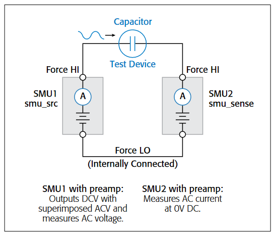
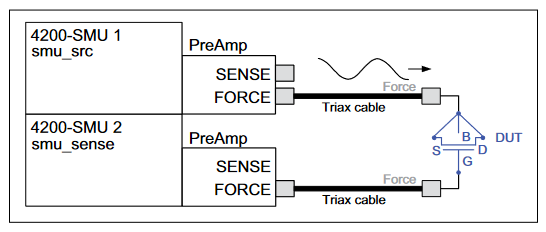
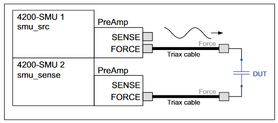
Figure 1 is a simplified diagram of the SMU instrument configuration used to generate the low frequency impedance measurements. This configuration requires a Model 4200-SCS system with two SMU instruments installed, with Model 4200-PA preamps connected to either side of the device under test. SMU1 outputs the DC bias with a superimposed AC signal and also measures the voltage. SMU2 measures the resulting AC current while sourcing 0V DC.
Basically, while the voltage is forced, voltage and current measurements are obtained simultaneously over several cycles. The magnitude and phase of the DUT impedance is extracted from the discrete Fourier transform (DFT) of a ratio of the resultant voltage and current sinusoids. This narrow-band information can be collected at varying frequencies (10mHz to 10Hz) to create a complex, multi-element model of the DUT. The resulting output parameters include the impedance (Z), phase angle (θ), capacitance (C), conductance (G), resistance (R), reactance (X), and the dissipation factor (D).
Because the very low frequency method works over a limited frequency range, the capacitance of the device under test (DUT) should be in the range of 1pF to 10nF. Table 1 summarizes the VLF C-V specifications (see Appendix A for complete specifications).
Table 1. Very Low Frequency C-V specifications
| Measurement Parameters | Cp, Gp, F, Z, θ, R, X, Cs, Rs, D, time |
| Frequency Range | 10mHz to 10Hz |
| Measurement Range | 1pF to 10nF |
| Typical Resolution | 3.5 digits, minimum typical 10fF |
| AC Signal | 10mV to 3V RMS |
| DC Bias | ±20V on the High terminal, minus the AC signal, 1µA maximum |
Required Hardware for VLF C-V Measurements
To make very low frequency impedance measurements, the following hardware is required:
- Model 4200-SCS with KTEI 9.0 or later software
- Two Model 4200 SMU instruments (Model 4200-SMU or Model 4210-SMU)
- Two Model 4200-PA Preamps
- Optional: Model 4210-CVU Capacitance Voltage Unit (for making high frequency C-V measurements)
Making Connections to the Device
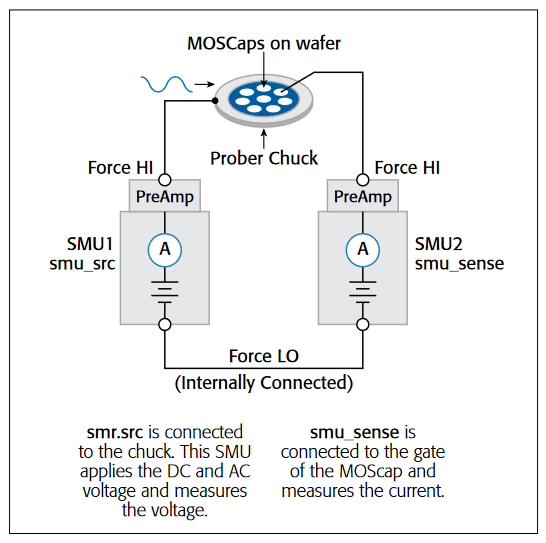
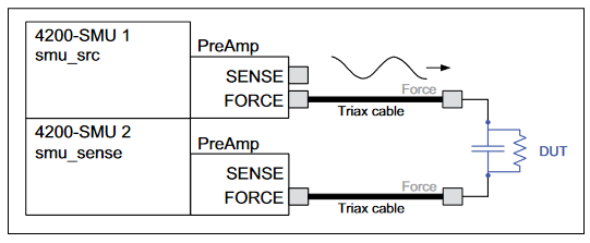
To make VLF C-V measurements on a device, connect the DUT between the two Force HI terminals of two SMU instruments (either Model 4200-SMU or Model 4210-SMU) with Model 4200-PA Preamps (Figures 1, 2). The preamp option is necessary because measuring very high impedances requires measuring very small currents. With the Model 4200-PAs, currents of <1E-12A can be measured. Because the VLF C-V method requires measuring small currents, it is best to use the triax cables that come with the SMU instruments to make these connections. The method does not support any switching instrumentation between the SMU instrument preamp and the device under test (DUT). One SMU outputs both the DC and AC voltage (SMU1 in Figures 1 and 2) and measures the AC voltage. The other SMU instrument measures the AC current (SMU2 in Figures 1 and 2). The SMU instrument used to measure the AC current should be connected to the high impedance terminal of the device (Figure 2).
An example of a MOSCap circuit connected for VLF C-V measurements is shown in Figure 2. Most MOSCaps have only a single pad on the top of the wafer, with the backside of the wafer used as the common contact for all MOSCaps. SMU1 outputs the AC+DC voltage and is connected to the chuck. The SMU that outputs the voltage is known as "smu_src" in the software that is included with the system. The high impedance terminal of the MOSCap is the gate and is connected to SMU2, which is called "smu_sense" in the software.
Using the KTEI Software to Perform VLF C-V Measurements
The system software includes five user modules and a project to make very low frequency C-V measurements. The user modules, listed in Table 2, are located in the VLowFreqCV User Library. The modules can be opened up as a User Test Module (UTM) within a project. KTEI 9.0 or later includes the VLF_CV_Examples project with the tests and results contained in the project (in the C:\s4200\kiuser\Projects\_CV project directory). This project (Figure 4) shows tests and data for a MOSFET, capacitor, MOSCap, and a test device consisting of a parallel RC combination. To run a test in the project, see "Testing a Device with VLF C-V."
Table 2. User Modules in the VLowFreqCV User Library.
| User Module | Description |
| vlfcv_measure | Measures C, G, Z, theta, R+jX at a fixed DC bias. |
| vlfcv_measure_dual_sweep_bias | Measures C, G, Z, theta, R+jX, time while sweeping the DC voltage. Optional dual sweep allows sweeping from dcv_bias_start to dcv_bias_stop, with 1 measure point at dcv_bias_stop, then back down to dcv_bias_start. |
| vlfcv_measure_dual_sweep_bias_fixed_range | Measures C, G, Z, theta, R+jX, time while sweeping the DC voltage. Measurements are made on a fixed current range which is determined by the expected_C, expected_R and maximum DC voltage. Optional dual sweep allows sweeping from dcv_bias_start to dcv_bias_stop, with 1 measure point at dcv_bias_stop, then back down to dcv_bias_start. |
| vlfcv_measure_sweep_freq | Measures C, G, Z, theta, R+jX, time at multiple user-specified test frequencies. |
| vlfcv_measure_sweep_time | Measures C, G, Z, theta, R+jX, time as a function of time. |
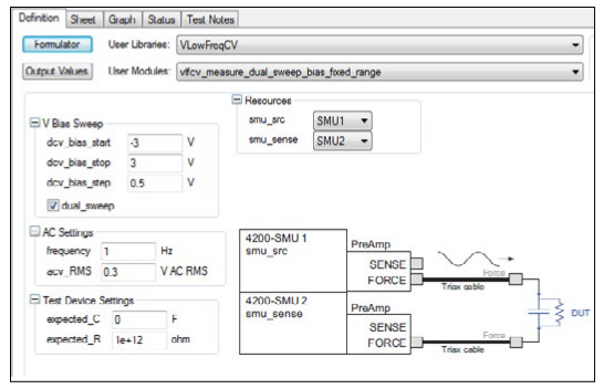
Once you've added a new module to a project, you need to input a few parameters. Many of the parameters are common to all five modules; however, each module has some unique parameters. Figure 3 illustrates the Definition tab of the vlfcv_measure_dual_sweep_bias_ fixed_range User Module showing all the user-defined parameters. The adjustable parameters for all the modules are listed in Tables 3 through 6.
The values of the expected capacitance (expected_C) and the expected parallel resistance (expected_R) determine which current range will be used to make the measurement. However, choosing specific values is generally not required, as setting expected_C = 0 will allow the test routines to estimate the C and R to use.
The simplest module is vlfcv_measure. It is used in the capacitor VLF_cap_one_ point test in the VLF_CV_Examples project. This test performs a single measurement. The module does not perform any sweeping, but it allows for all test parameters to be controlled (Table 3). Note that the maximum voltage possible is a combination of both the AC and DC voltages. The maximum negative DC bias voltage = -20 + (acv_RMS * √2 ). The maximum positive DC bias voltage = +20 - (acv_RMS * √2 ). Use expected_C = 0 to have the routine auto-detect the estimated C and R values.
Table 3. Adjustable parameters in vlfcv_measure User Module.
| Parameter | Range | Description |
| smu_src | SMUn | SMU instrument to source DC + AC voltage waveform and measure AC volts: SMU1, SMU2, SMU3… |
| smu_sense | SMUn | SMU t instrument o measure AC current: SMU1, SMU2, SMU3… |
| frequency | 0.01 to 10 | Test frequency in hertz, from 0.01 to 10. |
| Expected_C | 1e-12 to 1e-8 | Estimate of DUT capacitance in Farads, use 0 for auto-detect of DUT C and R. |
| Expected_R | 1e6 to 1e14 | Estimate of resistance parallel to DUT, in ohms |
| acv_RMS | 30e-3 to 3 | AC drive voltage in volts RMS |
| dcv_bias | ±20 less (acv_RMS * √2) | The DC voltage applied to the device |
Table 4. Adjustable parameters in the vlfcv_measure_dual_sweep_bias_fixed_range user modules.
| Parameter | Range | Description |
| smu_src | SMUn | SMU instrument to source DC + AC voltage waveform and measure AC volts: SMU1, SMU2, SMU3… |
| smu_sense | SMUn | SMU t instrument o measure AC current: SMU1, SMU2, SMU3… |
| frequency | 0.01 to 10 | Test frequency in hertz, from 0.01 to 10. |
| Expected_C | 1e-12 to 1e-8 | Estimate of DUT capacitance in Farads, use 0 for auto-detect of DUT C and R. |
| Expected_R | 1e6 to 1e14 | Estimate of resistance parallel to DUT, in ohms |
| acv_RMS | 30e-3 to 3 | AC drive voltage in volts RMS |
| dcv_start | ±20 less (acv_RMS * √2) | Starting DC voltage of the sweep |
| dcv_stop | ±20 less (acv_RMS * √2) | Stop DC voltage of the sweep |
| dcv_step | ±20 less (acv_RMS * √2) | Step size of the DC voltage. Number of steps limited to 512. |
| dual_sweep | 0 or 1 | Enter 0 for single sweep; enter 1 for dual sweep |
Table 5. Adjustable parameters in the vlfcv_measure_dual_sweep_freq user module.
| Parameter | Range | Description |
| smu_src | SMUn | SMU instrument to source DC + AC voltage waveform and measure AC volts: SMU1, SMU2, SMU3… |
| smu_sense | SMUn | SMU t instrument o measure AC current: SMU1, SMU2, SMU3… |
| frequency | 0.01 to 10 | Array of Test frequencies in Hertz.Maximum number of entries limited to 512, from 0.01 to 10. |
| Expected_C | 1e-12 to 1e-8 | Estimate of DUT capacitance in Farads, use 0 for auto-detect of DUT C and R. |
| Expected_R | 1e6 to 1e14 | Estimate of resistance parallel to DUT, in ohms |
| acv_RMS | 30e-3 to 3 | AC drive voltage in volts RMS |
| dcv_bias | ±20 less (acv_RMS * √2) | The DC voltage applied to the device |
Table 6. Adjustable parameters in the vlfcv_measure_sweep_time user module.
| Parameter | Range | Description |
| smu_src | SMUn | SMU instrument to source DC + AC voltage waveform and measure AC volts: SMU1, SMU2, SMU3… |
| smu_sense | SMUn | SMU t instrument o measure AC current: SMU1, SMU2, SMU3… |
| frequency | 0.01 to 10 | Test frequency in hertz, from 0.01 to 10. |
| Expected_C | 1e-12 to 1e-8 | Estimate of DUT capacitance in Farads, use 0 for auto-detect of DUT C and R. |
| Expected_R | 1e6 to 1e14 | Estimate of resistance parallel to DUT, in ohms |
| acv_RMS | 30e-3 to 3 | AC drive voltage in volts RMS |
| dcv_bias | ±20 less (acv_RMS * √2) | The DC voltage applied to the device |
| num_points | 1 to 512 | Number of points to take as a function of time |
Once the test is executed, several test parameters will be returned to the Sheet tab and can be saved as an .xls file. These test parameters can also be plotted on the Graph tab. Table 7 lists the returned test parameters and their descriptions. From these returned test parameters, more device extractions can be performed using the mathematical functions in the Formulator.
Note that the tests return all typical C-V measurement parameters. For example, both Cp-Gp and Cs-Rs are always returned, even if the test device response only matches the parallel model (Cp-Gp).
Table 7. Measurements returned for the modules in the VLowFreqCV library.
| Returned Test Parameters | Description |
| Status | Error code from test module execution. Definitions of the returned errors are listed at the bottom of the Definition tab in the UTM Description |
| times | Calculated time difference between readings. |
| dcv_bias | Programmed DC voltage applied to the device. |
| meas_Cp | Measured capacitance in parallel model (Cp-Gp). |
| meas_Gp | Measured conductance in parallel model (Cp-Gp) |
| meas_freq | Measured test frequency. |
| meas_Z | Measured impedance (Z-theta) |
| meas_Theta | Measured phase angle in degrees (Z-theta). |
| meas_R | Real component of the impedance (R + jX). |
| meas_X | Imaginary component of the impedance (R + jX). |
| meas_Cs | Measured AC capacitance in series model (Cs-Rs). |
| meas_Rs | Measured resistance in series model (Cs-Rs). |
| meas_D | Calculated dissipation factor, D. |
| meas_irange | The SMU instrument current range that the measurement was taken. |
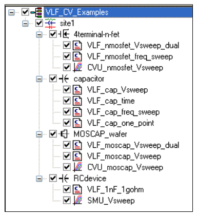
Using the VLF_CV_Examples Project
The VLF_CV_Examples project that comes with KTEI 9.0 or later has examples of VLF C-V measurements on various devices.This project is located in the "_CV" folder in the 4200 projects directory (c:\S4200\projects\_CV). The project has several UTMs that employ the user modules in the VLowFreqCV library.The project tree of the VLF_CV_Examples project is shown in Figure 4. The project contains tests for making both low frequency C-V measurements using the VLF C-V technique and also high frequency C-V measurements using the Model 4210-CVU Capacitance Voltage Unit. It also has one I-V test for initial screening of leakage current for test devices with unknown characteristics.
Even though the project has tests for specific devices, the VLF C-V user modules can be used on a variety of devices. The particular devices measured in the project are an n-MOSFET (gate to source/drain/bulk), a capacitor, a MOScap, and a parallel RC combination.
MOSFET
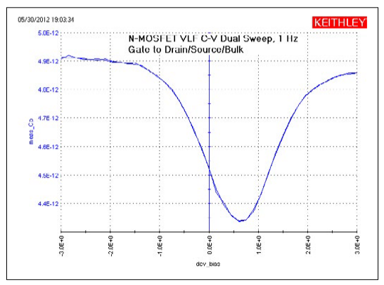
In the VLF_CV_Examples project, there are three tests for the n-fet devices: two UTMs and one ITM. Figure 6 shows the results of generating a very low frequency dual C-V sweep on an n-MOSFET measured between the Gate terminal and the Drain/Source/Bulk terminals tied together (Figure 5). This C-V sweep is in the VLF_nmosfet_Vsweep_dual UTM. Tests for measuring capacitance as a function of frequency (VLF_nmostfet_ freq_sweep), as well as a high frequency C-V test (CVU_nmostfet_ freq_sweep, taken with the Model 4210-CVU) are also included in the project.
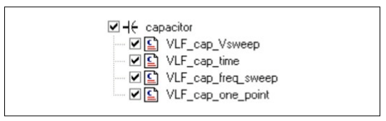
Capacitor
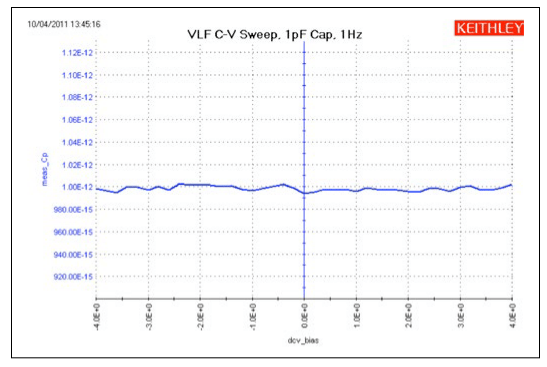
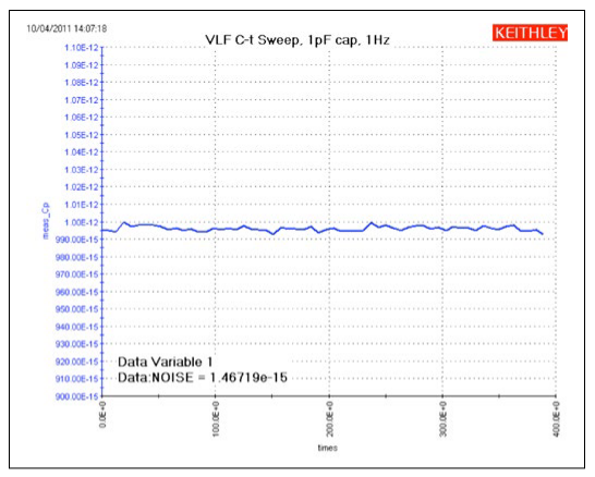
Using the VLF C-V method, capacitors can be measured in the range of 1pF to 10nF. The project has four UTMs (Figure 7).The VLF_cap_time UTM example in the project measures the capacitance of a 1pF capacitor as a function of time Figure 4. Project tree of VLF_CV_Examples project (Figure 10). The results of measuring the 1pF capacitor are shown in Figure 9. This small capacitance was measured at a test frequency of 1Hz with capacitance measurement noise levels at less than ±5E-15F. The Formulator can be used to determine the noise and average capacitance readings easily.
MOScap
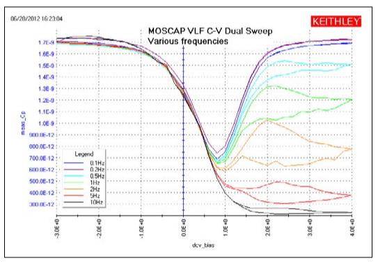
The MOScap device has three tests; all are DC bias sweeps with two using SMUs for the VLF C-V test DC bias voltage sweep (VLF_moscap_Vsweep_dual and VLF_moscap_Vsweep) and the other using the 4210-CVU for higher frequency testing (CVU_moscap_Vsweep). An example of a MOScap VLF-CV dual sweep generated with various test frequencies ranging from 0.1 Hz to 10 Hz is shown in Figure 11. This test was performed on a chuck at room temperature. This sweep is the result of executing the VLF_moscap_Vsweep_dual UTM in the project. From the low frequency C-V data, characteristics about the MOScap can be determined. The built-in math functions are helpful in performing the analysis of these devices from the C-V data. The connection diagram for the MOSCap is shown in Figure 2. The dual sweep functionality aids in determining any hysteresis behavior in the inversion region of the MOScap device, where frequency dependence is also observed. Note that the SMU instrument measuring the low current is not connected to the chuck. Connecting the sensitive (i.e., low-current measurement) instrument to the chuck will result in noisier measurements.
In addition to the UTM that generates VLF C-V measurements on the MOScap, the project includes an ITM to measure high frequency C-V on the MOScap. The high frequency C-V measurements were generated using the Model 4210-CVU, which has a test frequency range of 1kHz to 10MHz, with the example data taken at 100kHz.
To compare the results of both low and high C-V measurements on one graph, the data can be copied from one test module into another. Just select and copy the C-V measurements from the Sheet tab of one test module and then paste the data into the columns of the CALC Sheet of the other test module.The data in the CALC Sheet can be selected on the graph to plot.To do this, make sure to check the "Enable Multiple Xs" box in the Graph Definition window. An example showing both the low and high frequency C-V measurements on one graph is shown in Figure 12.
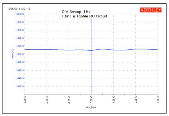
Parallel RC Device
Some devices can be modeled as a parallel RC combination (connection diagram in Figure 13). The parallel resistance is usually the leakage resistance of the device. There are two tests for the RC device: one is the UTM for a VLF C-V DC bias sweep (VLF_1nf _1gohm) and the other is an ITM V sweep (SMU_Vsweep). Figure 14 shows the results of performing a low frequency sweep on a 1.5nF and 1GW parallel combination.From the bias voltage and the resistance (1/Gp) of the device,the current was calculated in the Formulator and displayed on the graph. Excessive leakage current can cause erroneous results if the current exceeds the maximum current range for the particular RC combination. To determine the DC leakage current of an unknown DUT, use the ITM SMU_Vsweep, as described in the section titled "Testing a Device with VLF C-V." More information about making optimal results is described in the next section of this note.
Testing a Device with VLF C-V
Dissipation Factor
The parallel resistance of the device under test is a key aspect that determines the quality of the capacitance measurement because it causes additional DC current to flow, which reduces measurement accuracy. This parallel resistance at a given frequency is otherwise expressed as D, the dissipation factor.Here is the equation for the simple parallel model.
D = Reactance/Resistance = 1/ωRC = 1/2pfRC
where:
f is the test frequency, in Hz
R is the parallel resistance of the test device, in Ω
C is the capacitance of the test device, in farads
Guidance for measurement performance across a range of D values is shown in Table 8. As the table shows, higher D values reduce the accuracy of the reported C measurement.
"Not Recommended" means that the typical error is >10%.For details on specific capacitance and frequency values, see the VLF C-V Typical Specifications in Appendix A.
If the device is purely capacitive (very low to almost no leakage current, a D <0.1), then just connect the DUT as shown in Figure 8 (or Figure 2 if the DUT is on a wafer). After connection, run the desired test(s). However, if the device type is new, or its electrical characteristics are unknown, then use the following procedure. This procedure provides a guideline for determining reasonable parameter values for unknown test devices using the parallel model (Figure 13). It also provides guidance for evaluating results.
Table 8. VLF C-V typical accuracy vs. D and current measure range for the sense SMU instrument.
| 0.01 D | 0.1 D | 1 D | 10 D | |
| 1 µA | 0.6 % | 1.6 % | Not Recommended | Not Recommended |
| 100 nA | 1.4 % | 10 % | Not Recommended | Not Recommended |
| 10 nA | 0.7 % | 4 % | 6 % | Not Recommended |
| 1 nA | 0.4 % | 2 % | 2.6 % | 3 % |
| 100 pA | 0.8 % | 0.6 % | 0.6 % | 2 % |
Setup
- Connect the DUT as shown in Figure 2. The connection must be direct with the supplied triax cables. No switching or Model 4225-RPMs may be in the cable path from the SMU instrument PreAmp to the DUT. The VLF C-V method utilizes low current measurements, so ensure that appropriate shielding and guarding are used. Use triax cable and eliminate, if possible, or minimize any unshielded or unguarded cable runs. For on-wafer measurements, use triax probe manipulators and guarded probe arms.
- Open the VLF_CV_Examples project (in c:\S4200\projects\_CV). Create a new version of the project by renaming it by using the menu option File | Save Project As.
- Choose the SMU instrument IV sweep, SMU_Vsweep, under the RCdevice node. Choose voltage start and stop values for the sweep that match the desired minimum and maximum DC bias voltages to be used for VLF C-V tests. This test will help determine if the DUT leakage is too high for repeatable,accurate results.
- Run the SMU_Vsweep test. Review the results on the graph or in the Sheet. For best results, the maximum current shouldcbe <±1µA. If the current >±1µA, reduce the bias voltages until the current <±1µA. Note these voltages for later testing.These voltages may need to be adjusted again as described later in this procedure.
- Next, choose the VLF_cap_ freq_sweep test, under the capacitor device in the project tree. Enter the desired test frequencies, using just five to ten points to span the desired frequency range. If only one test frequency is desired, use the single point test VLF_cap_one_ point instead. Use the default expected_C = 0 and expected_R = 1E+12. Use acv_RMS = 0.3V and dcv_bias = 0.0V. This test will help determine the dissipation factor D of the DUT.
- Run the VLF_cap_ freq_sweep test. Review the results in the Sheet. Review the value(s) in the meas_D column. If |meas_D| <1, then the results are reasonable for the test frequencies and DC bias values that had <±1µA with the SMU_Vsweep test. If |meas_D| <10 then results should be reasonable for dcv_bias = 0V. If |meas_D| >10, then this present implementation of VLF C-V may provide unacceptable results or results with fairly large errors (see Table 8). Note that reasonable values with a low D value at dcv_bias = 0 may provide larger errors as the DC bias is increased.
- Configure the desired test, such as the bias sweep VLF_cap_Vsweep (Table 4) or frequency sweep VLF_cap_ freq_sweep (Table 5). Use the voltage values determined in the previous step. As stated earlier, using expected_C = 0 will perform an auto-detect of both the C and R values. For the other parameters, follow the description in the table corresponding to the test (Tables 3 through 6).
- Run or append the test. Running the test (green triangle) will discard the previous test data. The
append button (yellow triangle just to the right of the green run icon) will keep the old data, allowing
for comparison across multiple tests. The test parameters used for each append are in the Settings tab
of the Sheet. For unknown or new devices, review the measurements to ensure that the results are
reasonable by evaluating the data in the Sheet as well as the plotted values.
- Review the plotted data, noting the overall shape and Y-axis values.
- Check the status returned from the test. Status = 0 means that the routine did not detect any errors, but the validity of the data must still be assessed; go to the next step. If there is a non-zero status value, refer to the Table 9 Error Codes to see the explanation and troubleshooting suggestions.
- In the Sheet, check the current measurement range used.The column meas_irange, located on the right side of the Sheet, shows the current measure range used for each point. If this range is 1E-6 (1µA) or lower, skip to the next step. If any of the measure range values is 10E-6 (10µA) or larger, the results for these rows are suspect. Change the DC bias voltage to reduce the current measure range used for the test. For example, when running a voltage bias sweep, reduce the start and stop voltage used, for example from ±5V to ±2V, and re-run the test. Verify that the new test uses a meas_irange 1E-6 (1µA) or lower, then compare the results to the previous run taken with the 10µA range. Generally, the results with the 1 µA range are more accurate.
- If the Y-axis scale shows the maximum of 7E22 or 70E21, then an overflow has occurred on one or
more measurements in the test. Review the data in the Sheet, in the meas_Cp column, for entries
of 70E21 or 7E22. There are a few causes of the overflow:
- If the overflow values are only at the start and end of the test, consider reducing the range of sweep values to omit the sweep points that cause the overflow values. Another option is to specify appropriate values for expected_C and expected R. Before choosing values for expected_C and expected_R, let's briefly explain how these values affect the test. If the overflow values are most or all of the rows in the meas_Cp column, it is possible that an incorrect measure range was used for the test. This means that the current measure range used for the test was too small for the test parameters and DUT. The measure range used for the test is contained in the meas_irange in the Sheet. The current measure range for the sense SMU instrument is based on the expected_C and expected_R values.
- To change the current measure range for a test, supply an expected_C value that is larger than the meas_Cp value. Review the values in the meas_Cp column and choose a representative, non-overflow value and use it to calculate the expected_C = 2 * chosen meas_Cp value.To choose a value for expected_R, review the meas_Gp column for a representative value. Set expected_R = 1/(2* chosen meas_Gp).
- If one or more of the meas_Cp values is negative:
- Ensure that the DUT connections are good.
- The D may be too high, or the DC current leakage is too high compared to the capacitance
- Review the Sheet for meas_D and meas_irange values.If D > ~10 and or meas_irange is ≥10nA, the results may have a larger error
- Consult Table 8. Compare the current measure range (in the meas_irange) column to the corresponding row in Table 8. Note that the higher D values are more difficult to test.
- Try one or more of the following adjustments: a) reduce the DC bias voltage; b) increase the acv_RMS = 0.3V; c) increase the test frequency
- If the meas_Cp values seem noisy or inconsistent,append several tests with identical parameter values and review the data. If the results are different across each run, this indicates that the system is operating at or near the noise floor, which means that the capacitance value of the test device is small, or the test device has a higher D value (Table 8)
- If none of these adjustments provides reasonable results, try a higher frequency C-V test using the 4210-CVU, if available
- Add tests, such as the capacitance vs. time (test VLF_cap_time) or more DC bias sweeps at additional test frequencies.Recall that data may be saved in .xls or .csv file formats by using the Save As button on the Sheet, or on the Graph tab by clicking the Graph Settings button in the upper right corner and choosing Save As.
Initial Screening of DUT characteristics
Table 9. VLF C-V error codes and descriptions
| Error Code | Description | Explanation and Troubleshooting Recommendation |
| 0 | Test executed with no errors | No software or operational errors were detected. |
| -16001 | smu_src is out of range | Specified SMU instrument is not available in the chassis. For example, if SMU5 is entered, but there are only four SMU instruments in the 4200 chassis, then this error will occur. Modify SMU instrument string to an available SMU instrument number: SMU1, SMU2, SMU3.. |
| -16002 | smu_sense is out of range | Specified SMU instrument is not available in the chassis. For example, if SMU5 is entered, but there are only four SMU instruments in the 4200 chassis, then this error will occur. Modify SMU instrument string to an available SMU number: SMU1, SMU2, SMU3 |
| -16003 | Frequency is out of range. | Ensure that the test frequency is within the range of 10mHz to 10Hz, inclusive |
| -16004 | acv_RMS is out of range | Make sure that the RMS voltage is within the range of 0.01V to 3.0V, inclusive |
| -16005 | dcv_bias is out of range | Modify the DC or AC voltage bias to ensure that the ±20V maximum is not exceeded. Maximum negative voltage = –20 + (AC voltage *) Maximum positive bias voltage = 20 – (AC voltage * √2) |
| -16006 | hold_time is out of range | This error is unused for the VLowFreqCV routines |
| -16007 | delay_time is out of range | This error is unused for the VLowFreqCV routines. |
| -16008 | Too few points per period | This error indicates that the test was aborted by the operator. |
| -16009 | Output array sizes are not equal, or are larger than 4096. | Make sure all output array sizes are the same value and are not greater than 4096. |
| -16010 | Over range indication detected. | Current measurement over-range occurred and returned values are set to 7E22 (70E21).Troubleshooting: Review the value in the meas_CP column of the Sheet, looking for the overflow values (7E22 or 70E21). Follow the process given in Step 8d. |
| -16011 | Results array size is less than the number of points in the sweep. | Increase the size of all output arrays to be equal to the number of points in the sweep |
| -16012 | Could not collect enough data to perform measurement. | Cannot estimate expected_C or expected_R.This error occurs only when expected_C = 0.Input a estimated non-zero value for expected_C.Review the meas_Cp values in the Sheet for non-overflow values. Set estimated_C = 2 * nonoverflow meas_Cp |
| -16013 | Unable to allocate memory. | This error is unused for the VLowFreqCV routines. |
| -16014 | Current range is out of range | This error is unused for the VLowFreqCV routines. |
| -16015 | Irange_sense and expected_C cannot be 0 at the same time | This error is unused for the VLowFreqCV routines. |
| -16016 | Expected_C is out of range | Expected_C must be 0 (auto-detect C) or between 1E-15 and 1E-3, inclusive. |
| -16017 | This test requires preamp is connected to smu_sense | Make sure preamp is connected to each SMU used in the test. If reconnecting preamps, run run KCON and choose "Update PreAmp and RPM Configuration" in the Tools menu. |
| -16018 | Invalid start, stop, step DC bias sweep values. | Correct the values for the voltage bias sweep.dcv_bias_step cannot be 0, unless dcv_bias_start = dcv_bias_stop. If dcv_bias_start = dcv_bias_stop, then dcv_bias_step must = 0 |
| -16019 | Output array sizes are less than number of points in sweep. | Increase the size of all output arrays to be equal to the number of points in the sweep. |
| -16020 | Invalid combination of start, stop, step dc bias sweep values. | Correct the values for the voltage bias sweep.dcv_bias_step cannot be 0, unless dcv_bias_start = dcv_bias_stop. If dcv_bias_start = dcv_bias_stop, then dcv_bias_step must = 0. |
Guidelines for Making Optimal Measurements and Troubleshooting Techniques
When making high impedance, very low frequency C-V measurements using the SMU instruments, various techniques must be used to optimize measurement accuracy. These techniques include implementing low current measurement practices and choosing the appropriate settings in the software.
Implementing Low Current Measurement Techniques
Because using the very low frequency impedance measurement method involves measuring picoamp to femtoamp current levels,low current measurement techniques must be implemented.Use the triax cables that come with the Model 4200-SCS, which are shielded and will allow making a guarded measurement, if necessary. To reduce the noise due to electrostatic interference,make sure the device is shielded by placing it in a metal enclosure with the shield connected to the Force LO terminal of the Model 4200-SCS. Detailed information on low current measurement techniques can be found in Keithley’s Low Level Measurements Handbook. Also, ensure that the triax cable is directly connected to the DUT or probe pins; do not use any switching matrix or Model 4225-RPM in the SMU instrument signal path.
Choosing the Correct "expected_C" and "expected_R" Values
In most cases, expected_C should be 0 and the expected_R = 1E12 (both are the default values). When expected_C = 0, the VLF C-V routine will determine estimated values for both C and R of the device under test. The estimated R and C values determine the SMU instrument measurement range. If these values are chosen incorrectly, measurement errors or measurement range overflow may result (see Table 9, error code -16010 for more information). However, in some cases, entering a non-zero estimated capacitance for expected_C may provide better results for higher D devices or larger DC bias tests. To calculate a value of expected_C, multiply a non-overflow value from the meas_Cp column by two and enter this value into the test definition expected_C.
To determine if a device is compatible with the present VLF C-V approach, measure the DC resistance of the DUT, performing an I-V test using the SMU_Vsweep test under the RCdevice of the project tree of the VLF_CV_Examples project. Use the same test voltages in the I-V sweep that will be used in the impedance measurements. Additionally, performing a single measurement (test VLF_cap_one_ point) or frequency sweep (test VLF_cap_freq_sweep) at a DC bias of 0V will determine the D of the device. Refer to Testing a Device with VLF C-V and Table 8 for additional information.
Conclusion
The Model 4200-SCS contains a tool for performing very low frequency C-V measurements using the SMU instruments and preamps. This method enables the user to perform low capacitance measurements at a precise test frequency in the range of 10mHz to 10Hz. The KTEI 9.0 or later software included with the system enables the user to execute these low impedance measurements easily and extract important parameters about the DUT. When combined with the Model 4210-CVU Capacitance Voltage Unit, the Model 4200-SCS offers the user a single system that can perform both high and low frequency measurements.
Using the Ramp Rate Method for Making Quasistatic C-V Measurements with the Model 4200-SCS Parameter Analyzer
Introduction
Capacitance-voltage (C-V) measurements are generally made using an AC measurement technique. However, some capacitance measurement applications require a DC measurement technique. These are called quasistatic C-V (or QSCV) measurements because they are performed at a very low test frequency, that is,almost DC. These measurements usually involve stepping a DC voltage and measuring the resulting current or charge. Some of the techniques used for quasistatic C-V measurements include the feedback charge method and the linear ramp method. The Model 4200-SCS Parameter Analyzer uses a new method, the ramp rate method, which employs two Model 4200-SMUs Source Measure Unit (SMU) Instruments with two Model 4200-PA PreAmps. The optional 4200-PA PreAmps are required because this test involves sourcing and measuring current in the picoamp range. The SMU instruments are used to source current to charge the capacitor, and then to measure the voltage, time, and discharge current.
The software calculates the capacitance as a function of voltage from the measured parameters and shows the curve on the Model 4200-SCS's display. The software to execute the ramp rate method is included in version 7.1 and higher of the Keithley Test Environment Interactive (KTEI) software. This application note describes how to implement and optimize quasistatic C-V measurements using the Model 4200-SCS and the ramp rate method. It assumes the reader is familiar with making I-V measurements with the Keithley 4200-SCS at the level outlined in the Model 4200-SCS Reference Manual.
Ramp Rate Method
Figure 1 illustrates the basic connection diagram for the ramp rate method. This configuration requires two 4200-SMUs with 4200-PAs connected to either side of the device under test. Because the ramp rate method works over a limited range, the capacitance of the device under test should be in the range of 1pF to about 400pF.
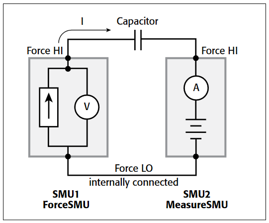
Basically, the ramp rate method works by charging up the device under test to a specific DC voltage using an SMU instrument as a current source. Once the device is charged up, a current of the opposite polarity is forced to discharge the device as the SMU instrument measures voltage as a function of time. A second SMU instrument measures the discharge current. From the measured voltage (V), current (I) and time (t) values, the capacitance (C) is derived as a function of voltage and time:
The ramp rate method included with the 4200-SCS follows these steps when making QSCV measurements:
- Charge the Device: A precharge current of 100pA is applied to the DUT by an SMU instrument, called ForceSMU, until the compliance voltage is reached. The compliance voltage is user specified and is called VStart. The polarity of the precharge current is the same as the polarity of the VStart voltage. If the precharge current is not sufficient to force the device to VStart, then a timeout error will be generated.
- Bias the Device for Specified Time Prior to Sweep: The device is biased at the VStart voltage for a user specified time (PreSoakTime) prior to the sweep.
- Apply Ramp Current to Discharge Device: Once the device is biased for a specified time,
a ramp rate current is applied to the device to discharge the device. The ramp rate current is of the
opposite polarity as the precharge current.The value of the ramp current is:
Iramp = CVal × RampRate
where:
CVal = the estimated capacitance value input by the user in farads (F).
RampRate = user input slope of stimulus voltage (dV/dt) in V/s.
- Simultaneously Trigger SMU Instruments to Take Measurements: The SMU instrument that is the ForceSMU measures voltage (V1, V2, T3 … Vn) and time (T1, T2, T3...Tn). The SMU instrument that is the MeasureSMU measures the current (I1, I2, I3 … In). The voltage, time, and current measurements are made until the opposite polarity of the VStart voltage is reached.
- Calculate Voltage, Time, and Capacitance Output Values: In real time, parameters are
extracted from the measurements and will appear in the Sheet or Graph. These parameters are
Vout = voltage, Tout = time, and Cout = capacitance, and are calculated
as follows:
Vout = (the average of two measured voltages)
Tout = T2 (the time when the second measurement is made)
Cout
where dV = V2 – V1 and dT = T2 – T1.
How to Make QSCV Measurements Using the KITE Software
The system's software includes a module to make quasistatic C-V measurements using the ramp rate method. This module, meas_qscv, located in the QSCVulib user library, can be opened up as a UTM from within a project.
Setting up the Parameters in the meas_qscv Module
Once you've opened the module up into a project, you need to input a few parameters. The adjustable parameters for the meas_qscv module are listed in Table 1.
Table 1. List of Adjustable Parameters in meas_qscv Module
| Parameter | Range | Description |
| ForceSMU | 1-8 | SMU instrument number that will force current through capacitive load. This SMU instrument must have a preamp. |
| MeasureSMU | 1-8 | SMU instrument number that will measure current. This SMU instrument must have a preamp. |
| VStart | -200 to 200 | Starting and ending voltages (V) for C-V sweep. |
| CVal | 1E–12 to 400E–12 | Approximate capacitance of device under test in Farads (F). |
| RampRate | 0.1 to 1 | Slope of stimulus voltage (dV/dt) in V/s. |
| PreSoakTime | 0 to 60 | Additional time delay in seconds to allow DUT, fixture, and cables to charge up. |
| TimeOut | 10 to 60 | Time allowed in seconds to charge up prior to time out. |
Here's a more detailed description of the input parameters:
ForceSMU: The SMU instrument that will force current to the device under test and measure the voltage as a function of time. This SMU instrument must have a preamp because it will be sourcing current in the picoamp range.
MeasureSMU: The SMU instrument that will measure the current flow in the circuit. This SMU instrument must have a preamp because it will be measuring current in the picoamp range.
VStart: This is both the starting and ending voltage of the C-V sweep because the C-V sweep is always symmetrical about 0V.
CVal: Enter at least the approximate maximum capacitance value of the device under test. This value is used to determine the magnitude of the source current to charge the device.
RampRate: The slope of the stimulus voltage in V/s. If the ramp rate is too fast, there will not be enough data points in the sweep. If the ramp rate it too slow, the readings may be noisy. Some experimentation may be needed to find the optimal setting for a particular device.
PreSoakTime: The length of time in seconds to apply the VStart voltage to the device prior to the start of the C-V sweep. Specify sufficient time for the device to charge up and reach equilibrium.
TimeOut: The amount of time allowed to charge the device to the VStart voltage until the test module times out. In some cases, such as when a device is shorted, the device may not reach the VStart voltage; this parameter enables the module to stop automatically and generate an error message. By default, this is set to 10 seconds.
Executing the Test
The meas_qscv module can be opened up in a project using a UTM (User Test Module). However, Keithley has already created a project called qscv that makes quasistatic C-V measurements using this module. It can be found at the following address on the Model 4200-SCS's hard drive:
C:\S4200\kiuser\Projects\_CV
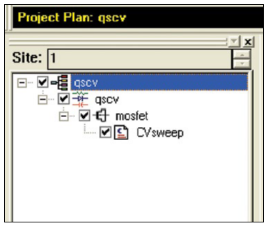
The project tree for the qscv project is shown in Figure 2.
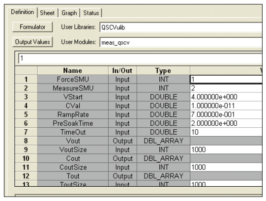
This project contains a UTM called CVsweep for making C-V measurements on a MOSFET device. The Definition Tab of CVsweep UTM is shown in Figure 3.
In this UTM, SMU1 (ForceSMU) and SMU2 (MeasureSMU) are used to make the C-V measurements. The VStart value is set to 4V, so this will generate a voltage sweep from –4V to 4V. The approximate capacitance value is 10pF, so this was entered as the CVal parameter. This CVal capacitance value will be used to determine the ramp rate current. If this number is too low (for example, 1E–12 instead of 10E–12), then the capacitance measurements will appear noisy. The RampRate value was set to 0.7V/s. In this case, a RampRate that is larger (1V/s) will produce a somewhat quieter curve but will have fewer data points. A RampRate that is smaller (0.1V/s) will produce a much noisier curve with lots of data points. You will need to experiment in order to determine the optimal settings for a particular device under test.
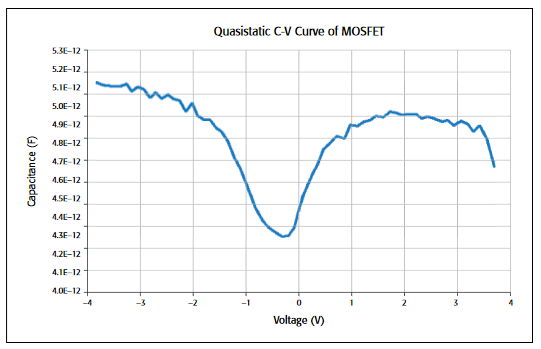
Once the device is connected to the two SMU instruments and the UTM is created with the desired input parameters, the C-V sweep can be executed. The results of such as sweep are shown in Figure 4.
Optimizing Measurements
When making quasistatic C-V measurements using the ramp rate method, various techniques must be used to optimize measurement accuracy. These techniques include implementing low current measurement practices and choosing the appropriate settings in the software.
Because using the ramp rate method involves sourcing and measuring picoamp-level current, low current measurement techniques must be implemented. Use the triax cables that come with the 4200-SCS, which are shielded and will allow making a guarded measurement. To reduce noise due to electrostatic interference, make sure the device is shielded by placing it in a metal enclosure with the shield connected to the Force LO terminal of the 4200-SCS. Detailed information on low current measurement techniques can be found in Keithley’s Low Level Measurements Handbook.
The parameter settings in the meas_qscv module that will most affect the measurements are CVal and RampRate. CVal is the approximate value of the device under test. If you input a value that is larger than that of the actual device, then the RampRate will be larger and there will be fewer data points. Conversely, if the capacitance value entered is smaller than the actual device capacitance, the RampRate will be lower and there will be more data points in the curve. Use the largest RampRate possible, but ensure the device curve appears settled. However, if the RampRate is too fast, there may not be enough points in the sweep.
To reduce the noise level of the curve, the moving average (MAVG) function in the Formulator can be used. Try using a moving average of three readings to see if this helps. Do not set the moving average number so large so that you lose the shape of your C-V curve.
To subtract the offset due to the cables and probe station, generate a C-V sweep using the meas_qscv module with the probes up or with an open circuit in the test fixture. Using the Formulator, take an average of the readings. Subtract this average offset value from capacitance measurements taken on the device under test.
Conclusion
Quasistatic C-V measurements can be made with the 4200-SMUs using the ramp rate method. This technique is implemented in software in the meas_qscv module of the QSCV_uslib user library of the 4200 KITE software. Using low level measurement techniques and choosing the appropriate parameter settings in the software will ensure optimal results.
Using the Model 4200-CVU-PWR C-V Power Package to Make High Voltage and High Current C-V Measurements with the Model 4200-SCS Parameter Analyzer
Introduction
Traditional capacitance-voltage (C-V) testing of semiconductor materials is typically limited to about 30V and 10mA DC bias. However, many applications, such as characterizing C-V parameters of LD MOS structures, low k interlayer dielectrics, MEMs devices, organic TFT displays, and photodiodes, require higher voltage or higher current C-V measurements. For these applications, a separate high voltage DC power supply and a capacitance meter are required to make the measurements.
The Model 4200-CVU-PWR C-V Power Package for the Model 4200-SCS allows making C-V measurements with a DC voltage bias of up to ±200V or 400V differential (0 to ±400V) and a current output of up to 300mA. Using this package, the Model 4200-CVU Capacitance-Voltage Unit measures the capacitance and either one or two 4200-SMUs (or 4210-SMUs for current up to 300mA) are used to supply the DC bias or sweep voltage. The C-V Power Package includes two bias tees that enable coupling of the AC signals from the 4200-CVU and the DC signals from the 4200-SMU. Along with the hardware, the C-V Power Package includes interactive software to control the high voltage C-V measurements using the KITE software. This application note explains how to implement and optimize high voltage C-V tests using the Model 4200-CVU-PWR C-V Power Package. It assumes the reader is familiar with making C-V measurements with the Keithley 4200-SCS with the 4200-CVU at the level outlined in [1] and [2].
Making Connectons To The Device
The Model 4200-CVU-PWR C-V Power Package comes with two Model 4205-RBT Remote Bias Tees. The desired voltage output will determine if one or two bias tees are required in the test circuit. For C-V measurements with an applied voltage bias up to ±200V, one bias tee is required. For C-V measurements with a voltage differential up to 400V (for example: 0 to 400V or –100 to 300V), two bias tees are required.
To make C-V measurements with an applied voltage bias up to ±200V, one 4200-SMU Source Measure Unit (SMU) Instrument, one 4200-CVU Capacitance-Voltage Unit, and one 4205-RBT Remote Bias Tee are connected to the device as shown in Figure 1. The 4200-SMU sources the DC voltage and the 4200-CVU measures the capacitance of the device under test (DUT). The 4205-RBT allows coupling of the AC signals from the CVU and the DC signal from the SMU instrument.
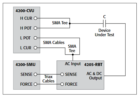
In this setup, either the CVL1 (LPOT and LCUR) or CVH1 (HPOT and HCUR) can be connected to the AC Input of the bias tee. By default, the AC ammeter is connected to the CVL1 terminals and it is best that the AC ammeter be connected to the gate of the device if applicable. If this is the case, then the HCUR and HPOT (or CVH1) terminals of the 4200-CVU are connected to the other side of the device or to the chuck. The DC bias is supplied by the 4200-SMU, with the Force and Sense from the SMU instrument connected to the Force and Sense terminals of the bias tee. The SMU LO terminals and the CVU CVH1 terminals are referenced internally to the system output common.
For C-V measurements that require up to 400V differential, two Model 4205-RBT Remote Bias Tees and two 4200-SMUs are required in addition to the 4200-CVU Capacitance Voltage Unit. This configuration is shown in Figure 2. Using this configuration, 4200-SMU 1 and the CVL1 terminals of the 4200-CVU are connected through one 4205-RBT Remote Bias Tee to one side of the device. The other side of the device is connected through a second 4205-RBT bias tee to both the 4200-SMU 2 and the CVH1 terminals of the 4200-CVU. This setup allows 400V differential measurements, for example, 0 to 400V, –100 to 300V, or –400V to 0V.
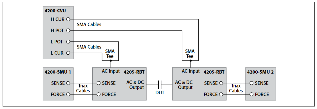
Using the KITE Software to Control High Voltage C-V Measurements
The hivcvulib user library contains two modules, SweepV and CvsT, for controlling the high voltage C-V measurements. These modules can be used with either the one or two bias tee configurations.
Using one bias tee, the SweepV module allows the user to sweep a DC voltage across the DUT using the 4200-SMU and measure the capacitance using the 4200-CVU. If two bias tees are used with the SweepV module, then one SMU instrument is used to sweep the DC voltage and the other SMU instrument is used to apply an offset DC bias (as shown in Figure 2).
The CvsT module provides capacitance measurements as a function of time at a user-specified DC bias. This module can also be used with either one or two bias tees. With one bias tee and one SMU instrument, capacitance measurements can be made with up to 200V DC bias. With two bias tees and two SMU instruments, capacitance measurements can be made up to 400V DC.
These modules can be opened up in a project using a User Test Module (UTM). However, a project has already been created that uses these test modules. This project, called CVU_highV, can be found at the following location on the 4200-SCS:
C:\S4200\kiuser\Projects\_CV
The CVU_highV project uses both the SweepV and CvsT modules to make measurements on devices.
Setting up the Parameters in the SweepV Module
Table 1 lists the adjustable parameters for the SweepV module.This module has settings for the 4200-CVU and up to five 4200-SMUs in the test circuit. One SMU instrument is used for the voltage sweep in the C-V measurements. Up to four other SMU instruments can be used to output a DC bias. One SMU instrument can also be used to measure current.
Table 1. List of Adjustable Parameters in SweepV module
| Parameter | Range | Description |
| OpenCompensate | 0 or 1 | Enables/Disables Open Compensation for CVU. |
| ShortCompensate | 0 or 1 | Enables/Disables Open Compensation for CVU. |
| CVUCableLen | 0, 1.5m, 3m | Set cable length for CVU |
| SweepSMU | 1-8 | SMU instrument number that will force voltage in C-V sweep |
| MeasISMU | 1-8 | SMU instrument number that will measure current during the C-V sweep |
| StartV | –200 to +200 | Step voltage for sweep |
| StopV | –200 to +200 | Step voltage for sweep |
| StepV | –200 to +200 | Step voltage for sweep |
| SweepDelay | 0 to 10 seconds | Time between voltage steps |
| PresoakV | –200 to +200 | Voltage bias prior to start of sweep |
| PresoakTime | 0 to 600 seconds | Time to apply soak voltage |
| SMU1Bias | –200 to +200 | Voltage forced by SMU1 during sweep (ignored with SMU1 is SweepSMU) |
| SMU2Bias | –200 to +200 | Voltage forced by SMU2 during sweep (ignored with SMU2 is SweepSMU) |
| SMU3Bias | –200 to +200 | Voltage forced by SMU3 during sweep (ignored with SMU3 is SweepSMU) |
| SMU4Bias | –200 to +200 | Voltage forced by SMU4 during sweep (ignored with SMU4 is SweepSMU) |
| Frequency | 10e3 to 10e6 | Test frequency |
| ACVoltage | 0.01 to 0.1V | AC test voltage of CVU |
| Speed | 0 fast, 1 normal, 2 quiet | Speed of CVU |
| CVRange | 0=Auto, 1µA, 30µA, 1mA | CVU measure range |
Here is a description of the input parameters:
OpenCompensate: If desired, an offset correction can be performed. First, go to the Tools Menu and select CVU Connection Compensation. Then click on the Measure Open button. After this compensation procedure is performed, it can be enabled in this module by setting the OpenCompensate parameter value to 1.
ShortCompensate: For lower impedance devices, a short compensation should be performed. This is especially true for the two bias tee configuration. First, short the CVH1 and CVL1 terminals. In the Tools Menu, select CVU Connection Compensation and then click on the Measure Short button.After this compensation procedure is performed, short compensation can be enabled in the SweepV module by setting the ShortCompensate parameter value to 1.
CVUCableLen: Input the length of the CVU cables. By default, this is set to 1.5m, the length of the SMA cables that come with the 4200-CVU, Keithley P/N CA-447A.
SweepSMU: This is the number of the SMU instrument that will force the sweep voltage in the C-V sweep. The Force HI and Sense HI terminals of this SMU instrument are connected to the Force and Sense terminals of the Model 4205-RBT Remote Bias Tee.
MeasISMU: The user inputs the number of the SMU instrument that will measure current in the circuit. If the SMU instrument that is measuring current is not the SMU instrument that is used to sweep voltage (SweepSMU), then the current range is set to limited autorange to the 100nA range. If the SMU instrument that is measuring current is the same as the SweepSMU, then the current range is set to limited autorange on the 10µA range. If this is the case, additional sweep delay time needs to be added to ensure a settled reading. It also may be necessary to use PreSoakV and PreSoakTime to charge up the device to the first step in the sweep prior to taking the current measurements.
StartV, StopV, StepV: Input the start, stop, and step size voltages for the C-V sweep.
SweepDelay: The time between steps in the voltage sweep.Allow an adequate delay time to ensure the device reaches equilibrium. If measuring current through the bias tee, additional SweepDelay time may need to be added to ensure optimal results.
PreSoakV: This is the voltage bias output by the SweepSMU prior to the start of the voltage sweep.
PresoakTime: This is the length of the time in seconds for the PreSoakV voltage to be applied to the device. You can verify how much time is required for the device to reach equilibrium by using the CvsT module in the hivcvulib. This module measures the capacitance as a function of a time while the device is biased with a constant DC voltage. The settling time can be observed from the graph.
SMU1Bias, SMU2Bias, SMU3Bias, SMU4Bias: In addition to an SMU instrument supplying a voltage for the C-V sweep, up to four more SMU instruments can be used to bias other parts of the test circuit.
Frequency: Test frequency of CVU, which can be set to 10kHz, 20kHz, 30kHz, 40kHz, 50kHz, 60kHz, 70kHz, 80kHz, 90kHz, 100kHz, 200kHz, 300kHz, 400kHz, 500kHz, 600kHz, 700kHz, 800kHz, 900kHz, 1MHz, 2MHz, 3MHz, 4MHz, 5MHz, 6MHz, 7MHz, 8MHz, 9MHz, and 10MHz. For higher capacitance values, the test frequency may need to be lowered through the bias tee to avoid errors due to resonance.
ACVoltage: The amplitude of the AC voltage output of the CVU.
Speed: The speed time can be set as: 0 = FAST, 1 = NORMAL, and 2 = QUIET. The FAST mode has the fastest time but the highest noise. The NORMAL mode is the most common setting,which allows sufficient settling times for most measurements.The QUIET mode ensures high accuracy but a slower settling time. The QUIET mode allows more time for DC settling and provides longer integration time.
Here is a description of the input parameters for the CvsT module:
OpenCompensate: If desired, an offset correction can be performed. First, go to the Tools Menu and select CVU Connection Compensation. Then click on the Measure Open button. After this compensation procedure is performed, it can be enabled in this module by setting the OpenCompensate parameter value to 1.
ShortCompensate: For lower impedance devices, a short compensation should be performed. This is especially true for the two bias tee configuration. First, short the CVH1 and CVL1 terminals. In the Tools Menu, select CVU Connection Compensation and then click on the Measure Short button.After this compensation procedure is performed, short compensation can be enabled in the CvsT module by setting the ShortCompensate parameter value to 1.
CVUCableLen: Input the length of the CVU cables. By default, this is set to 1.5m, the length of the SMA cables that come with the 4200-CVU, Keithley P/N CA-447A.
MeasISMU: The user inputs the number of the SMU instrument that will measure current in the circuit. The current range is set to limited autorange to the 100nA range.SampleCount: Enter the number of capacitance measurements from 1 to 10000.
Interval: This is the time between readings in seconds.SMU1Bias, SMU2Bias, SMU3Bias, SMU4Bias: Up to four SMU instruments can be used to bias the test circuit. One or two of these SMU instruments is connected through a bias tee(s) to supply voltage to the DUT for the C-V measurement.
Frequency: Test frequency of CVU which can be set to 10kHz, 20kHz, 30kHz, 40kHz, 50kHz, 60kHz, 70kHz, 80kHz, 90kHz, 100kHz, 200kHz, 300kHz, 400kHz, 500kHz, 600kHz, 700kHz, 800kHz, 900kHz, 1MHz, 2MHz, 3MHz, 4MHz, 5MHz, 6MHz, 7MHz, 8MHz, 9MHz, and 10MHz. For higher capacitance values, the test frequency may need to be lowered through the bias tee to avoid errors due to resonance.
ACVoltage: The amplitude of the AC voltage output of the CVU.Speed: The speed time can be set as: 0 = FAST, 1 = NORMAL, and 2 = QUIET. The FAST mode has the fastest time but the highest noise. The NORMAL mode is the most common setting, which allows sufficient settling times for most measurements.The QUIET mode ensures high accuracy but a slower settling time. The QUIET mode allows more time for DC settling and provides longer integration time.
CVRange: This is the AC ammeter measurement range of the CVU. The input values are 0 for autorange, 1µA, 30µA, and 1mA ranges.
Applications for High Voltage Capacitance Measurements
Even though the user can set up new UTMs for testing many types of devices, the CVU_highV project comes with UTMs already configured for four types of devices: zener diodes, MOScaps, capacitors, and Schottky diodes. The project tree for the CVU_highV project is shown in Figure 3. A description of the specific tests follows.
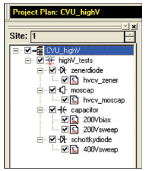
Zener Diode Testing
To make high voltage C-V measurements on a zener diode, connect the zener diode to the 4200 system as shown in Figure 4. In this configuration, the anode is connected to the CVH1 terminals of the 4200-CVU and the cathode is connected to the AC and DC Output terminal of the 4205-RBT Remote Bias Tee. This connects the Force and Sense HI terminals of the SMU instrument (DC bias) and the AC ammeter of the CVU to the cathode.
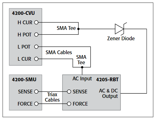
The UTM for testing zener diodes is called hvcv_zener. This UTM is set up to reverse bias the zener diode from 0 to 180V in 1V steps. The capacitance as a function of voltage is plotted in the Graph tab. For displaying the capacitance and voltage measurements over a wide range, a log-log or semi-log graph can be generated instead. The C-V measurement results of a 1N5388A zener diode are shown in Figure 5.
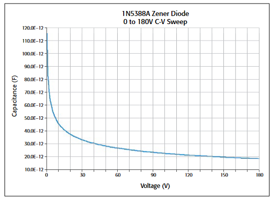
MOScap Testing
The connections for making high voltage capacitance-voltage measurements on a MOScap are shown in Figure 6. In this application, the LPOT and LCUR (or CVL1) are connected to the AC Input of the bias tee. By default, the AC ammeter is internally connected to the CVL1 terminals, and it is best that the ammeter be connected to the gate of the device as shown. The HCUR and HPOT (CVH1) terminals of the 4200-CVU are connected to the chuck. The DC bias is supplied by the 4200-SMU, which gets connected to the gate through the bias tee. Connecting the Force HI terminal of the SMU instrument to the gate through the bias tee will ensure the proper polarity of the gate voltage.
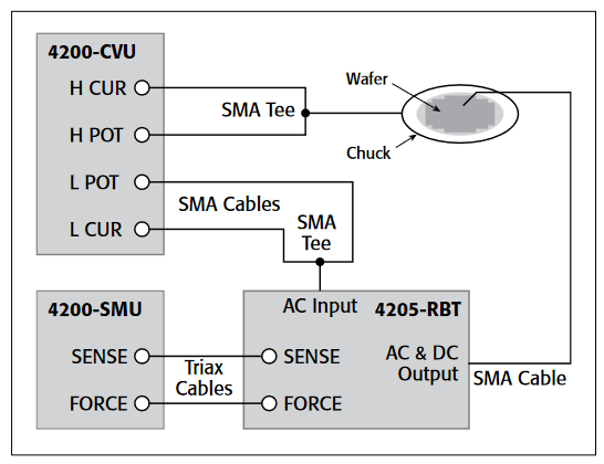
The UTM for performing high voltage C-V measurements on MOScaps is called hvcv_moscap and is located under the "moscap" device in the project tree. This UTM sweeps the gate voltage from 10V to –90V in 0.5V steps. The results are graphed as shown in Figure 7.
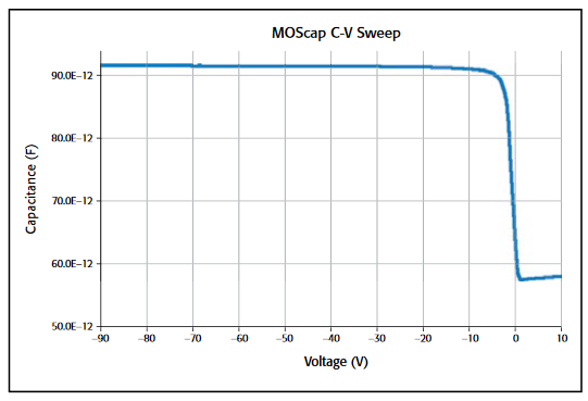
Once the C-V measurements are made, various MOScap parameters can be derived. The hvcv_moscap UTM includes formulas for extracting several parameters including threshold voltage, oxide thickness, flatband capacitance, doping concentration, etc. These parameters are calculated in the Formulator and the calculated values appear in the Sheet tab.These formulas are listed in Table 3. The specific details about these formulas can be found in Keithley Application Note Number 2896, "C-V Characterization of MOS Capacitors Using the Model 4200-SCS Parameter Analyzer."
In addition to the equations for the derived parameters in the Formulator, several constants have been added to the Constants Table in the Formulator. These constants are listed in Table 4.The user will need to adjust these constants in the Formulator based on the MOScap device being tested.
Table 4. Constants for hvcv_moscap UTM
| Constant | Description | Default Value | Units |
| AREA | Gate Area of Device | 10.8E-3 | cm2 |
| EOX (εox) | Permittivity of Oxide | 340.0E-15 | F/cm |
| ES (εs) | Semiconductor Permittivity | 1.04E-12 | F/cm |
| NI (Ni) | Intrinsic Carrier Concentration | 14.5E+09 | cm-3 |
| DOPETYPE | –1 for 1 for P-type, N-type | 1E+00 | |
| WM (WM) | Metal Work Function | 4.15E+00 | V |
| WS (WS) | Silicon Electron Affinity | 4.05E+00 | V |
| EBG (EBG) | Semiconductor Energy Gap | 1.12E+00 | eV |
| TEMP | Test Temperature | 293E+00 | K |
Capacitor Testing
Two test modules exist for testing capacitors: one applies a constant 200V bias and the other sweeps the voltage from –200V to 200V. To perform these tests, the capacitor is connected to the test system using one bias tee as previously shown in Figure 1.
High voltage capacitance vs. time measurements can be made using the 200vbias UTM, which was created using the CvsT module. This module applies 200V to a 100pF capacitor, measures the capacitance as a function of time, and plots the data in the graph. The results are shown in Figure 8. This module can be used to determine how much settling time to use during an actual C-V sweep.
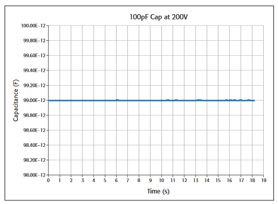
In the 200Vsweep UTM, the CVU measures the capacitance while an SMU instrument sweeps the test voltage from –200V to +200V. The results of the C-V sweep of the 100pF capacitor are shown in Figure 9.
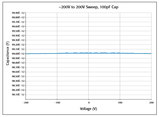
Schottky Diode Testing
Using two bias tees and two SMU instruments, C-V measurements can be made up to 400V. An example of this configuration is shown in Figure 10. In this setup, the 4200-CVU, two 4205-RBTs, and two 4200-SMUs are connected to a Schottky diode.In the 400Vsweep UTM, capacitance measurements are made as a 0 to 400V sweep is generated across a Schottky diode. To generate the 0 to 400V sweep, SMU1 sweeps from –200V to 200V while SMU2 outputs a constant –200V bias. This results in a high voltage C-V sweep as shown in the graph in Figure 11.
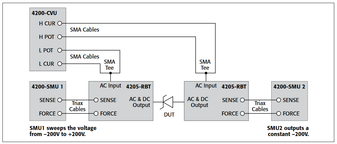
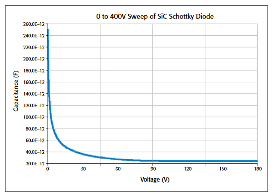
Optimizing Measurements
When making high voltage C-V measurements, as with making C-V measurements in general, various techniques can be used to optimize measurement accuracy. These techniques include choosing the proper speed modes, allowing sufficient settling time, and taking steps to reduce the effects of stray capacitance.
The two modules in the hivcvulib library include an adjustable Speed parameter. The Speed parameter can be set as: 0 = FAST, 1 = NORMAL, and 2 = QUIET. The FAST mode has the fastest time but the highest noise. The NORMAL mode is the most common setting, which allows sufficient settling times for most measurements. The QUIET mode ensures high accuracy but a slower settling time. The QUIET mode allows more time for DC settling and provides longer integration time.
Choosing an appropriate PreSoak Time and SweepDelay Time is important for many applications. The condition of a device when all internal capacitances are fully charged after an applied step voltage is referred to as "equilibrium." If capacitance measurements are made before a device is in equilibrium, inaccurate results may be produced. To choose the delay times for the SweepV module, make a measurement of capacitance vs. time in the CvsT module. Observe the settling time on the graph. Use this time as the PresoakTime for the PreSoakV or the SweepDelay time applied to each step in the sweep in the SweepV module.
When making C-V measurements, it is important to take steps to reduce the effects of stray capacitance, which include offset compensation and proper connections.
To correct for offsets, use Open and Short Compensation.Open Compensation corrects for large impedance, small capacitance offsets. Short Compensation corrects for low impedance, high capacitance offsets. Open and Short Compensation are explained in greater detail in Section 15 of the Model 4200-SCS Reference Manual.
To avoid noisy measurements and stray capacitance, the AC ammeter terminal (LCUR) should always be connected to the terminal of the device that has the least amount of capacitance to ground. When measuring MOScaps, always connect the CVL1 terminals (LCUR and LPOT) to the gate and the CVH1 terminals (HCUR and HPOT) to the chuck.
Because the bias tee unavoidably adds some external parasitics to the measurement circuit, care must be taken when making measurements especially at higher capacitances using higher test frequencies (>1MHz). If measurement errors are suspected, make C-V measurements without the bias tee, and then make measurements through the bias tee with the same test conditions (frequency, voltage, speed, interval time, etc.). The measurements without the bias tee are made using an ITM and will be limited to ±30V. If there are discrepancies, try lowering the test frequency, if possible, and use the Quiet speed mode.Increasing the settling time may ensure the device has reached equilibrium
Test System Safety
Many electrical test systems or instruments are capable of measuring or sourcing hazardous voltage and power levels. It is also possible, under single fault conditions (e.g., a programming error or an instrument failure), to output hazardous levels even when the system indicates no hazard is present. These high voltage and power levels make it essential to protect operators from any of these hazards at all times. Protection methods include:
- Design test fixtures to prevent operator contact with any hazardous circuit.
- Make sure the device under test is fully enclosed to protect the operator from any flying debris.
- Double insulate all electrical connections that an operator could touch. Double insulation ensures the operator is still protected, even if one insulation layer fails.
- Use high reliability, fail-safe interlock switches to disconnect power sources when a test fixture cover is opened.
- Where possible, use automated handlers so operators do not require access to the inside of the test fixture or have a need to open guards.
- Provide proper training to all users of the system so they understand all potential hazards and know how to protect themselves from injury.
It is the responsibility of the test system designers, integrators, and installers to make sure operator and maintenance personnel protection is in place and effective.
Conclusion
Using the Model 4200-CVU-PWR C-V Power Package for the Model 4200-SCS allows making C-V measurements with a DC voltage bias of up to ±200V or 400V differential and a current output of up to 300mA. To achieve the higher test voltage and current, this package couples the AC and DC signals from the 4200-CVU and 4200-SMU (or 4210-SMU) using the Model 4205-RBT Remote Bias Tees. Software that allows making either high voltage C-V sweeps or capacitance measurements at a constant DC voltage is included with the package. Example tests are included for a zener diode, MOS capacitor, capacitor, and Schottky diode. These tests can be easily modified to measure other devices or new tests can be created by opening a UTM in another project. Like C-V measurements in general, high voltage C-V measurements require using appropriate measurement techniques and connections to ensure optimal results.
Measuring Inductance Using the 4200-CVU Capacitance-Voltage Unit
Introduction
Although the 4200-CVU capacitance option for Keithley's Model 4200 Parameter Analyzer does not measure inductance directly, users can easily extract the inductance from the parameters it does measure: impedance (Z), phase angle (theta or θ), and the test frequency (f). This application note describes how users of the Model 4200-SCS can determine inductance using the 4200-CVU option.
Equipment Requirements
This application requires the use of a Model 4200-SCS system with the 4200-CVU option installed. Although the procedure given here does not depend on the use of a specific KTEI version, 4200-CVU is only supported by KTEI version 7.0 and later.
Implementation procedure
The formulas for deriving the inductance are as follows:
| X = | Z |
| sinθ |
where:
X = Reactance
Z = Impedance
θ = Phase angle between capacitance and conductance C,G (rads)
| L = | X |
| 2πf |
where:
L = Inductance
X = Reactance
π = Archimedes constant (3.141592…)
f = Test frequency
To incorporate these formulas into a KITE project:
- Create an Interactive Test Module (ITM) and choose the 4200-CVU (CVH1 and CVL1) for the measurements at the device terminals in the ITM.
- In the Force Function/Measure Options window, set the Measured Options Parameters to "Z,Theta" as shown in Figure 1.
- Open the Formulator and type in the formula for the reactance using the Data Series parameters Z, Theta, and F.The units for "Theta" are in degrees. To use the trigonomic functions in the Formulator, you must convert the units to rads using the "RAD" function as shown in Figure 2 for a device with terminals A and B:
- Type in the formula for inductance from X and F. "Pi" (π) can be found in the constants area of the Formulator.
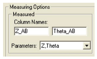
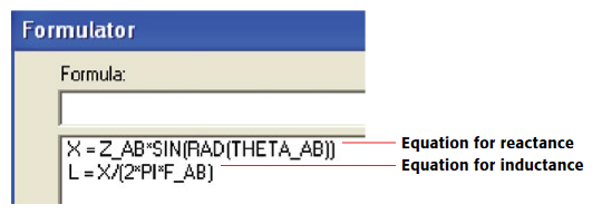
Example results
Once the project is saved and executed, the inductance (L) will appear in the Sheet tab as shown in Figure 3. It can also be plotted on a graph.
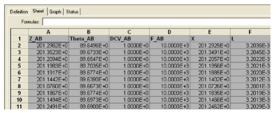
Other considerations and possible sources of error
This method is useful for measuring inductances ranging from microhenries to millihenries. The actual range that can be measured and the quality of the results achieved will depend on the characteristics of the specific device under test-its own impedance, etc.—and the instrument settings, such as the test frequency.
According to the inductance equation, use lower frequencies to measure higher inductances and vice versa.
Standard best practices for high quality electrical measurements should be used, including the use of four-wire connections as close to device as possible, etc.
Electrical Characterization of Photovoltaic Materials and Solar Cells with the Model 4200-SCS Parameter Analyzer
I-V, C-V, C-f, DLCP, Pulsed I-V, Resistivity, and Hall Voltage Measurements
Introduction
The increasing demand for clean energy and the largely untapped potential of the sun as an energy source is making solar energy conversion technology increasingly important.As a result, the demand for solar cells, which convert sunlight directly into electricity, is growing. Solar or photovoltaic (PV) cells are made up of semiconductor materials that absorb photons from sunlight and then release electrons, causing an electric current to flow when the cell is connected to a load.A variety of measurements are used to characterize a solar cell's performance, including its output and its efficiency. This electrical characterization is performed as part of research and development of photovoltaic cells and materials, as well as during the manufacturing process.
Some of the electrical tests commonly performed on solar cells involve measuring current and capacitance as a function of an applied DC voltage. Capacitance measurements are sometimes made as a function of frequency or AC voltage.Some tests require pulsed current-voltage measurements.These measurements are usually performed at different light intensities and under different temperature conditions. A variety of important device parameters can be extracted from the DC and pulsed current-voltage (I-V) and capacitance-voltage (C-V) measurements, including output current, conversion efficiency, maximum power output, doping density, resistivity, etc. Electrical characterization is important in determining how to make the cells as efficient as possible with minimal losses.
Instrumentation such as the Model 4200-SCS Parameter Analyzer can simplify testing and analysis when making these critical electrical measurements. The Model 4200-SCS is an integrated system that includes instruments for making DC and ultra fast I-V and C-V measurements, as well as control software,graphics, and mathematical analysis capability. The Model 4200-SCS is well-suited for performing a wide range of measurements, including DC and pulsed current-voltage (I-V), capacitancevoltage (C-V), capacitance-frequency (C-f), drive level capacitance profiling (DLCP), four-probe resistivity (ρ, σ), and Hall voltage (VH) measurements. This application note describes how to use the Model 4200-SCS to make these electrical measurements on PV cells.
Making Electrical Measurements with the Model 4200-SCS
To simplify testing photovoltaic materials and cells, the Model 4200-SCS is supported with a test project for making many of the mostly commonly used measurements easily. These tests, which include I-V, capacitance, and resistivity measurements, also include formulas for extracting common parameters such as the maximum power, short circuit current, defect density, etc. The SolarCell project (Figure 1) is included with all Model 4200-SCS systems running KTEI Version 8.0 or later. It provides thirteen tests (Table 1) in the form of ITMs (Interactive Test Modules) and UTMs (User Test Modules) for electrical characterization
Table 1. Test modules in the SolarCell project
| Subsite Level | Test Module | Description |
| IV_sweep | fwd-ivsweep | Performs I-V sweep and calculates Isc,Voc, Pmax, Imax, Vmax, FF |
| rev-ivsweep | Performs reversed bias I-V sweep | |
| CV_sweep | cvsweep | Generates C-V sweep |
| C-2vsV | Generates C-V sweep and calculates 1/C2 | |
| cfsweep | Sweeps the frequency and measures capacitance | |
| DLCP | Measures capacitance as AC voltage is swept. DC voltage is applied so as to keep the total applied voltage constant.The defect density is calculated. | |
| Pulse-IV | pulse-iv-sweep | Performs pulse I-V sweep using one channel of PMU |
| 4PtProbe_resistivity | HiR | Uses 3 or 4 SMUs to source current and measure voltage difference for high resistance semiconductor materials.Calculates sheet resistivity. |
| LoR | Uses 1 or 2 SMUs to source current and measure voltage using remote sense.Calculates sheet resistivity. Uses current reversal method to compensate for thermoelectric voltage offsets. | |
| vdp_resistivity | I1_V23 | First of 4 ITMs that are used to measure the van der Pauw resistivity. This ITM sources current between terminals 1 and 4 and measures the voltage difference between terminals 2 and 3. |
| I2_V34 | Sources current between terminals 2 and 1 and measures the voltage difference between terminals 3 and 4. | |
| I3_V41 | Sources current between terminals 3 and 2 and measures the voltage difference between terminals 4 and 1. | |
| I4_V12 | Sources current between terminals 4 and 1 and measures the voltage difference between terminals 1 and 2. |
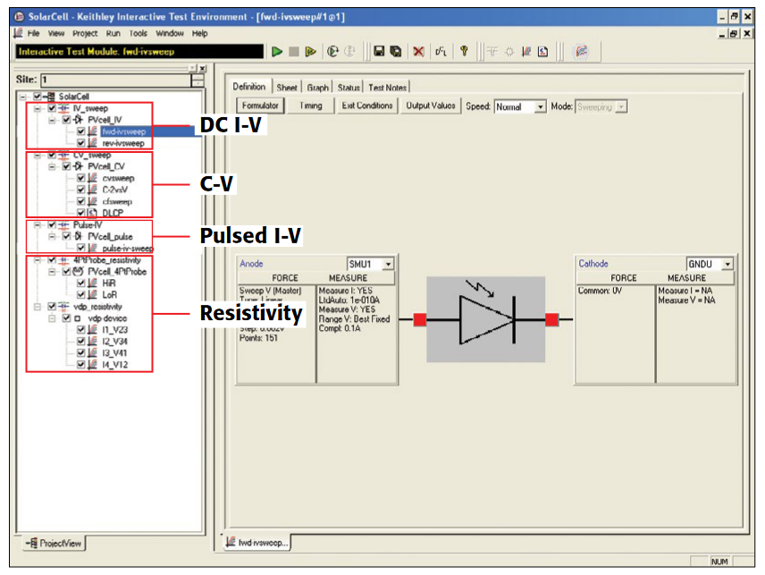
DC Current-Voltage (I-V) Measurements
As described previously, many solar cell parameters can be derived from current-voltage (I-V) measurements of the cell.These I-V characteristics can be measured using the Model 4200-SCS's source measure units (SMU) instruments, which can source and measure both current and voltage. Because these SMU instruments have four-quadrant source capability, they can sink the cell current as a function of the applied voltage.Two types of SMU instruments are available for the Model 4200-SCS: the Model 4200-SMU, which can source/sink up to 100mA, and the Model 4210-SMU, which can source/sink up to 1A. If the output current of the cell exceeds these current levels, it may be necessary to reduce it, possibly by reducing the area of the cell itself. However, if this is not possible, Keithley's Series 2400 or 2600B SourceMeter® SMU Instruments, which are capable of sourcing/sinking higher currents, offer possible alternative solutions.
Parameters Derived from I-V Measurements
A solar cell may be represented by the equivalent circuit model shown in Figure 2, which consists of a light-induced current source (IL), a diode that generates a saturation current [IS(eqV/kT –1)], series resistance (rs), and shunt resistance (rsh).The series resistance is due to the resistance of the metal contacts, ohmic losses in the front surface of the cell, impurity concentrations, and junction depth. The series resistance is an important parameter because it reduces both the cell’s shortcircuit current and its maximum power output. Ideally, the series resistance should be 0Ω (rs = 0). The shunt resistance represents the loss due to surface leakage along the edge of the cell or to crystal defects. Ideally, the shunt resistance should be infinite (rsh = ∞).
If a load resistor (RL) is connected to an illuminated solar cell, then the total current becomes:
I = IS(eqV/kT - 1) - IL
where:
IS = current due to diode saturation
IL = current due to optical generation
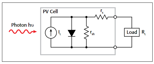
Several parameters are used to characterize the efficiency of the solar cell, including the maximum power point (Pmax), the energy conversion efficiency (η), and the fill factor (FF). These points are illustrated in Figure 3, which shows a typical forward bias I-V curve of an illuminated PV cell. The maximum power point (Pmax) is the product of the maximum cell current (Imax) and the voltage (Vmax) where the power output of the cell is greatest. This point is located at the "knee" of the curve.
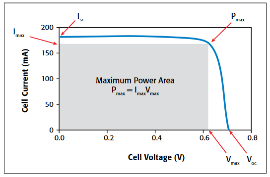
The fill factor (FF) is a measure of how far the I-V characteristics of an actual PV cell differ from those of an ideal cell. The fill factor is defined as:
| FF = | ImaxVmax |
| IscVoc |
where:
Imax = the current at the maximum power output (A)
Vmax = the voltage at the maximum power output (V)
Isc = the short-circuit current (A)
Voc = the open-circuit voltage (V)
As defined, the fill factor is the ratio of the maximum power (Pmax = ImaxVmax) to the product of the short circuit current (Isc) and the open circuit voltage (Voc). The ideal solar cell has a fill factor equal to one (1) but losses from series and shunt resistance decrease the efficiency.
Another important parameter is the conversion efficiency (η), which is defined as the ratio of the maximum power output to the power input to the cell:
| η = | Pmax |
| Pin |
where:
Pmax = the maximum power output (W)
Pin = the power input to the cell defined as the total radiant energy incident on the surface of the cell (W)
Making Connections to the Solar Cell for I-V Measurements
Figure 4 illustrates a solar cell connected to the Model 4200-SCS for I-V measurements. One side of the solar cell is connected to the Force and Sense terminals of SMU1; the other side is connected to the Force and Sense terminals of either SMU2 or the ground unit (GNDU) as shown.
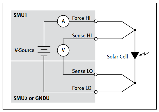
Using a four-wire connection eliminates the lead resistance that would otherwise affect this measurement’s accuracy. With the four-wire method, a voltage is sourced across the solar cell using one pair of test leads (between Force HI and Force LO), and the voltage drop across the cell is measured across a second set of leads (across Sense HI and Sense LO).The sense leads ensure that the voltage developed across the cell is the programmed output value and compensate for the lead resistance.
Forward-Biased I-V Measurements
Forward-biased I-V measurements of the solar cell are made under controlled illumination. The SMU instrument is set up to output a voltage sweep and measure the resulting current. This forward bias sweep can be performed using the "fwd-ivsweep" ITM, which allows adjusting the sweep voltage to the desired values. As previously illustrated in Figure 3, the voltage source is swept from V1 = 0 to V2 = VOC. When the voltage source is 0 (V1 = 0), the current is equal to the source-circuit current (I1 = ISC). When the voltage source is an open circuit (V2 = VOC), then the current is equal to zero (I2 = 0). The parameters, VOC and ISC, can easily be derived from the sweep data using the Model 4200-SCS's built-in mathematical analysis tool, the Formulator.For convenience, the SolarCell project has the commonly derived parameters already calculated, so the values automatically appear in the Sheet tab every time the test is executed. Figure 5 shows some of the derived parameters in the Sheet tab. These parameters include the short-circuit current (ISC), the open circuit voltage (VOC), the maximum power point (Pmax), the maximum cell current (Imax), the maximum cell voltage (Vmax), and the fill factor (FF).
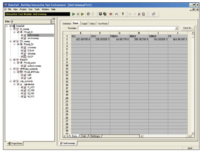
Th user can easily add other formulas depending on the required parameters that need to be determined.
Using the Formulator, the conversion efficiency (η) can also be calculated if the user knows the power input to the cell and inputs the formula. The current density (J) can also be derived by using the Formulator and inputting the area of the cell.
Figure 6 shows an actual I-V sweep of an illuminated silicon PV cell generated with the Model 4200-SCS using the "fwd-ivsweep" ITM. Because the system's SMU instruments can sink current, the curve passes through the fourth quadrant and allows power to be extracted from the device (I–, V+). If the current output spans several decades as a function of the applied voltage, it may be desirable to generate a semilog plot of I vs.V. The Graph tab options support an easy transition between displaying data graphically on either a linear or a log scale.
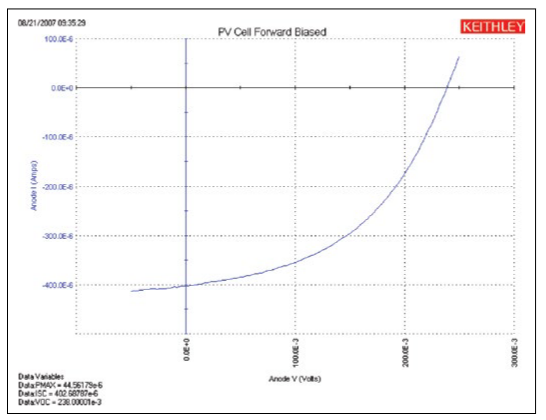
If desired, the graph settings functions make it easy to create an inverted version of the graph about the voltage axis. Simply go to the Graph Settings tab, select Axis Properties, select the Y1 Axis tab, and click on the Invert checkbox. The inverse of the graph will appear as shown in Figure 7.
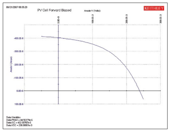
The series resistance (rs) can be determined from the forward I-V sweep at two or more light intensities. First, make I-V curves at two different intensities (the magnitudes of the intensities are not important). Measure the slope of this curve from the far forward characteristics where the curve becomes linear. The inverse of this slope yields the series resistance:
By using additional light intensities, this technique can be extended using multiple points located near the knee of the curves. As illustrated in Figure 8, a line is generated from which the series resistance can be calculated from the slope.
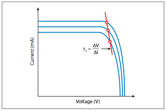
When considered as ammeters, one important feature of the Model 4200-SCS's SMU instruments is their very low en. The voltage burden is the voltage drop across the ammeter during the measurement. Most conventional digital multimeters (DMMs) will have a voltage burden of at least 200mV at full scale. Given that only millivolts may be sourced to the sample in solar cell testing, this can cause large errors. The Model 4200-SCS's SMU instruments don’t produce more than a few hundred microvolts of voltage burden, or voltage drop, in the measurement circuit.
Reverse-Biased I-V Measurements
The leakage current and shunt resistance (rsh) can be derived from the reverse-biased I-V data. Typically, the test is performed in the dark. The voltage is sourced from 0V to a voltage level where the device begins to break down. The resulting current is measured and plotted as a function of the voltage. Depending on the size of the cell, the leakage current can be as small as picoamps. The Model 4200-SCS has a preamp option that allows making accurate measurements well below a picoamp. When making very sensitive low current measurements (nanoamps or less), use low noise cables and place the device in a shielded enclosure to shield it electrostatically. This conductive shield is connected to the Force LO terminal of the Model 4200-SCS. The Force LO terminal connection can be made from the outside shell of the triax connectors, the black binding post on the ground unit (GNDU), or from the Force LO triax connector on the GNDU.
One method for determining the shunt resistance of the PV cell is from the slope of the reverse-biased I-V curve, as shown in Figure 9. From the linear region of this curve, the shunt resistance can be calculated as:
| rsh = | ∆VReverse Bias |
| ∆IReverse Bias |
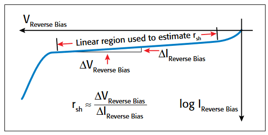
Figure 10 shows an actual curve of a reverse-biased solar cell, generated using the ITM "rev-ivsweep". In this semi-log graph, the absolute value of the current is plotted as a function of the reverse-biased voltage that is on an inverted x-axis.
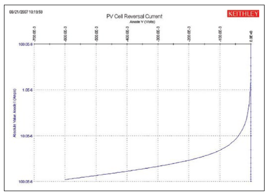
Capacitance Measurements
Capacitance-voltage measurements are useful in deriving particular parameters about PV devices. Depending on the type of solar cell, capacitance-voltage (C-V) measurements can be used to derive parameters such as the doping concentration and the built-in voltage of the junction. A capacitance-frequency (C-f) sweep can be used to provide information on the existence of traps in the depletion region. The Model 4210-CVU, the Model 4200-SCS's optional capacitance meter, can measure the capacitance as a function of an applied DC voltage (C-V), a function of frequency (C-f), a function of time (C-t), or a function of the AC voltage. The Model 4210-CVU can also measure conductance and impedance.
To make capacitance measurements, a solar cell is connected to the Model 4210-CVU as shown in Figure 11. Like I-V measurements made with the SMU instrument, the capacitance measurements also involve a four-wire connection to compensate for lead resistance. The HPOT/HCUR terminals are connected to the anode and the LPOT/LCUR terminals are connected to the cathode. This connects the high DC voltage source terminal of the Model 4210-CVU to the anode.
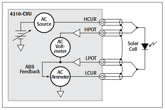
Figure 11 shows the shields of the four coax cables coming from the four terminals of the capacitance meter. The shields from the coax cables must be connected together as close as possible to the solar cell to obtain the highest accuracy because this reduces the effects of the inductance in the measure circuit.This is especially important for capacitance measurements made at higher test frequencies.
Performing an Open and Short Connection Compensation will reduce the effects of cable capacitance on measurement accuracy. This simple procedure is described in Section 15 of the Model 4200-SCS Reference Manual.
Given that the capacitance of the cell is directly related to the area of the device, it may be necessary to reduce the area of the cell itself, if possible, to avoid capacitances that may be too high to measure. Also, setting the Model 4210-CVU to measure capacitance at a lower test frequency and/or lower AC drive voltage will allow measuring higher capacitances.
C-V Sweep
C-V measurements can be made either forward-biased or reversebiased. However, when the cell is forward-biased, the applied DC voltage must be limited; otherwise, the conductance may get too high for the capacitance meter to measure. The maximum DC current cannot be greater than 10mA; otherwise, the instrument's DC voltage source will go into compliance and the DC voltage output will not be at the desired level.
Figure 12 illustrates a C-V curve of a silicon solar cell generated by the Model 4210-CVU using the "cvsweep" ITM. This test was performed in the dark while the cell was reversed-biased.
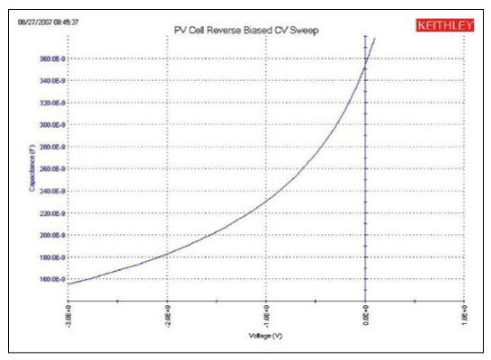
Rather than plotting dC/dV, it is sometimes desirable to view the data as 1/C2 vs. voltage because some parameters are related to the 1/C2 data. For example, the doping density (N) can be derived from the slope of this curve because N is related to the capacitance by:
| N(a) = | 2 |
| qESA2[d(1/C2)/dV] |
where:
N(a) = the doping density (1/cm3)
q = the electron charge (1.60219 × 10⁻¹⁹C)
Es = semiconductor permittivity (1.034 × 10⁻¹²F/cm for silicon)
A = area (cm2)
C = measured capacitance (F)
V = applied DC voltage (V)
The built-in voltage of the cell junction can be derived from the intersection of the 1/C2 curve and the horizontal axis. This plot should be a fairly straight line. An actual curve taken with the Model 4210-CVU, generated using the "C-2vsV" ITM, is shown in Figure 13. The Formulator function is used to derive both the doping density (N) and the built-in voltage on the x-axis (x-intercept). The doping density is calculated as a function of voltage in the Formulator and appears in the Sheet tab in the ITM. The user must input the area of the cell in the Constants area of the Formulator. The built-in voltage source value is derived both in the Formulator and by using a Linear Line Fit option in the Graph settings. Notice the value of the x-intercept appears in the lower left corner of the graph.
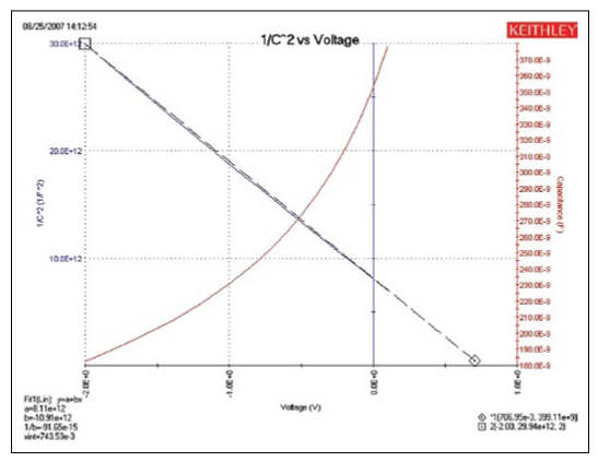
C-f Sweep
The Model 4210-CVU option can also measure capacitance, conductance, or impedance as a function of the test frequency.The range of frequency is from 1kHz to 10MHz. The curve in Figure 14 was generated by using the "cfsweep" ITM. Both the range of sweep frequency and the bias voltage can be adjusted. The desired parameters, such as the trap densities, can be extracted from the capacitance vs. frequency data. The measurements can be repeated at various temperatures.
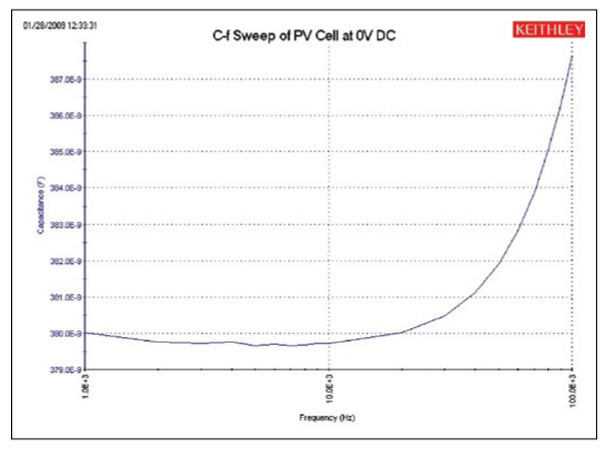
Drive Level Capacitance Profiling (DLCP)
Drive Level Capacitance Profiling (DLCP) is a technique for determining the defect density (NDL) as a function of depth of a photovoltaic cell1. During the DLCP measurement, the applied AC voltage (peak-to-peak) is swept and the DC voltage is varied while the capacitance is measured. This is in contrast to the conventional C-V profiling technique, in which the AC rms voltage is fixed and the DC voltage is swept.
In DLCP, the DC voltage is automatically adjusted to keep the total applied voltage (AC + DC) constant while the AC voltage is swept. By maintaining a constant total bias, the exposed charge density (ρe) inside the material stays constant up to a fixed location (xe), which is defined as the distance from the interface where EF - Ev = Ee. This is also in contrast to conventional C-V profiling, the analysis of which assumes that the only charge density changes occur at the end of the depletion region.
Thus, in DLCP, the position (xe) can be varied by adjusting the DC voltage bias to the sample. This also allows determining the defect density as a function of the distance, or special profiling.
The test frequency and temperature of the measurement can also be varied to show a profile that is energy dependent.
Once the measurements are taken, a quadratic fit of the C-V data is related to the impurity density at a given depletion depth as follows for a p-type semiconductor:
| NDL ≡ | C03 | = | ρe | = | P + ∫EF0Ev + Ee g(E,Xe)dE |
| 2qεA2C1 | q |
where:
NDL = defect density (cm-3)
C1, C0 = coefficients of quadratic fit of C-V data
q = electron charge (1.60 × 10⁻¹⁹C)
ε = permittivity (F/cm)
A = area of solar cell (cm2)
ρe = charge density (C/cm3)
p = hole density (cm-3)
xe = distance from interface where EF - Ev = Ee
The coefficients C0 and C1 are determined via a full leastsquares best fit of the data to a quadratic equation:
dQ/dV = C2(dV)2 + C1*(dV) + C0
However, only the C0 and C1 coefficients are used in the analysis.
The "DLCP" UTM allows making C-V measurements for drive level capacitance profiling. During these measurements, the total applied voltage remains constant as the DC voltage bias is automatically adjusted as the AC voltage drive level amplitude varies. The AC amplitude of the 4210-CVU can vary from 10mVrms to 100mVrms (14.14mV to 141.4mVp-p). The range of frequency can also be set from 1kHz to 10MHz. The capacitance is measured as the AC voltage is sweeping.
Table 2 lists the input parameters used in the UTM, the allowed range of input values, and descriptions. The user inputs the total applied voltage (VmaxTotal), the AC start, stop, and step voltages (VacppStart, VacppStop, and VacppStep), the time between voltage steps (SweepDelay), the test frequency (Frequency), the measurement speed (Speed), the measurement range (CVRange), and offset compensation (OpenComp,ShortComp, LoadComp, and LoadVal).
Table 2. Adjustable parameters for the DLCP UTM
| Parameter | Range | Description |
| VmaxTotal | -10 to 10 volts | Applied DC Volts and ½ AC Volts p-p |
| VacppStart | .01414 to .1414 | Start Vac p-p |
| VacppStop | .02828 to .1414 | Start Vac p-p |
| VacppStep | .0007070 to .1414 | Start Vac p-p |
| SweepDelay | 0 to 100 | Sweep delay time in seconds |
| Frequency | 1E+3 to 10E+6 | Test Frequency in Hertz |
| Speed | 0, 1, 2 | 0=Fast, 1=Normal, 2=Quiet |
| CVRange | 0, 1E–6, 30E–6, 1E–3 | 0=autorange, 1µA, 30µA, 1mA |
| OpenComp | 1, 0 | Enables/disables open compensation for CVU |
| ShortComp | 1, 0 | Enables/disables short compensation for CVU |
| LoadComp | 1, 0 | Enables/disables load compensation for CVU |
| LoadVal | 1 to 1E+9 | Load value |
Once the test is executed, the capacitance, AC voltage, DC voltage, time stamp, frequency, and the defect density (NDL) are determined and their values are listed in the Sheet tab. The defect density is calculated in the Formulator using a quadratic line fit of the C-V data. The coefficients (C0 and C1) of the quadratic equation are also listed in the Sheet tab. The user inputs the area and permittivity of the solar cell to be tested into the Constants/Values/Units area of the Formulator.
Figure 15 shows the measurement results in the graph of capacitance vs. AC voltage p-p. Notice the coefficients of the derived quadratic line fit and the defect density are displayed on the graph.
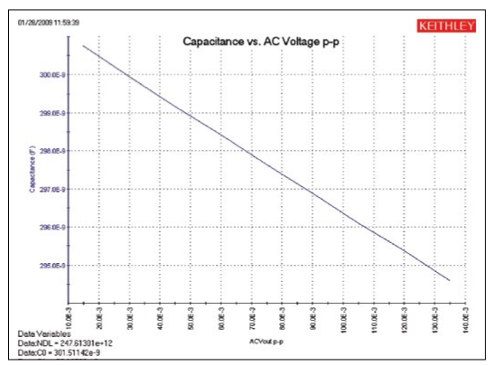
The capacitance measurements can be repeated at various applied total voltages in order to vary the position of xe. The energy (Ee) can be varied by changing the test frequency (1kHz to 10MHz) or the temperature. To change the temperature of the measurement, the user can add a User Test Module (UTM) to control a temperature controller via the Model 4200-SCS's GPIB interface. The Model 4200-SCS is provided with user libraries for operating the Temptronics and Triotek temperature controllers.
Pulsed I-V Measurements
Pulsed I-V measurements can be useful for studying parameters of solar cells. In particular, pulsed I-V measurements have been used to determine the conversion efficiency, minimum carrier lifetime, and the effects of cell capacitance. The Model 4225-PMU, the Model 4200-SCS's optional Ultra-Fast I-V Module, can output pulsed voltage and measure current, and can capture ultrahigh-speed current or voltage waveforms in the time domain. In addition to sourcing a pulsed voltage, the PMU can sink current so it can measure a solar cell’s current output.
To make pulsed I-V measurements on a solar cell, the Model 4225-PMU is connected to the cell as shown in Figure 16. Each PMU has two channels so the solar cell can be connected using either one or two channels. In the one-channel case shown, one end of the cell is connected to the HI terminal of PMU CH1 and the other side of the cell is connected to the shield of the coax cable, which is the LO terminal of the PMU.
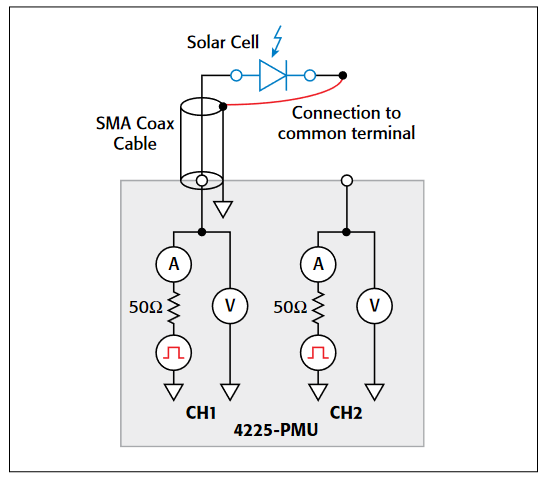
Unlike the DC I-V and C-V measurements, the 4225-PMU uses a two-wire technique. The Short Compensation feature can be used to "zero out" the voltage drops due to the cables so that a 4-wire measurement technique isn't necessary.
Because solar cells are fairly capacitive, it is important to ensure the pulse width is long enough for the pulsed I-V sweep.The waveform capture mode should be used to verify the pulse width prior to generating the pulsed I-V sweep. The waveform capture mode enables a time-based current and/or voltage measurement that is typically the capture of a pulsed waveform.This can be used to perform a dynamic test on the cell or used as a diagnostic tool for choosing the appropriate pulse settings in the pulsed I-V mode. Given that larger solar cells have larger capacitances, it may be necessary to reduce the area of the cell itself to avoid a long settling time in the measurement.
The results of generating a pulsed I-V measurement sweep on a silicon solar cell are shown in Figure 17. Note that the current is in the fourth quadrant of the curve. This indicates that the PMU is sinking current; in other words, the current is flowing out of the solar cell and into the PMU.
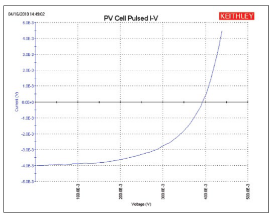
Resistivity and Hall Voltage Measurements
Determining the resistivity of a solar cell material is a common electrical measurement given that the magnitude of the resistivity directly affects the cell's performance. Resistivity measurements of semiconductor materials are usually performed using a four-terminal technique. Using four probes eliminates errors due to the probe resistance, spreading resistance under each probe, and the contact resistance between each metal contact and the semiconductor material. Two common techniques for determining the resistivity of a solar cell material are the fourpoint collinear probe method and the van der Pauw method.The SolarCell project contains several ITMs for making both types of measurements. More detailed information about making resistivity measurements on semiconductor materials using the Model 4200-SCS can be found in Keithley Application Note #2475, "Four-Probe Resistivity and Hall Voltage Measurements with the Model 4200-SCS."
Four-Point Collinear Probe Measurement Method
The four-point collinear probe technique involves bringing four equally spaced probes in contact with a material of unknown resistance. The probe array is placed in the center of the material as shown in Figure 18. The two outer probes are used to source current and the two inner probes are used to measure the resulting voltage difference across the surface of the material.
From the sourced current and the measured voltage, the surface or sheet resistivity is calculated by:
| σ = | Π | × | V |
| ln2 | I |
where:
σ = surface resistivity (W/■)
V = the measured voltage (V)
I = the source current (A)
Note that the units for sheet resistivity are expressed as ohms per square (W/■) in order to distinguish this number from the measured resistance (V/I), which is simply expressed in ohms.Correction factors to the resistivity calculation may be required for extremely thin or thick samples or if the diameter of the sample is small relative to the probe spacing.
If the thickness of the sample is known, the volume resistivity can be calculated as follows:
| ρ = | Π | × | V | × | t | × | k |
| ln2 | I |
where:
ρ = volume resistivity (Ω-cm)
t = the sample thickness (cm)
k = a correction factor* based on the ratio of the probe spacing to wafer diameter and on the ratio of wafer thickness to probe spacing
* The correction factors can be found in a standard four-point probe resistivity test procedure such as Semi MF84: Standard Test Method for Measuring Resistivity of Silicon Wafers With an In-Line Four-Point Probe. This standard was originally published by ASTM International as ASTM F 84.
Using the Four-Point Probe ITMs, HiR and LoR
The "HiR" and "LoR" ITMs are both used for making four-point collinear probe measurements. The "HiR" ITM can be used for materials over a wide resistance range, ~1mΩ to 1TΩ.The Model 4200-PA preamps are required for making high resistance measurements (>1MΩ). The "LoR" ITM is intended for measurements of lower resistance materials (~1mΩ - 1kΩ).
A screenshot of the "HiR" ITM for measuring four-probe resistivity is shown in Figure 19.
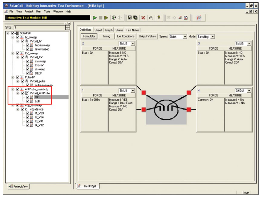
The "HiR" ITM uses either three or four SMU instruments to make the resistivity measurements. One SMU instrument (SMU1) and the ground unit (GNDU) are used to source current between the outer two probes. Two other SMU instruments (SMU2 and SMU3) are used to measure the voltage drop between the two inner probes. The Force HI terminal of each SMU instrument is connected to each of the four probes. The SMU instrument designation for this configuration is shown in Figure 20.
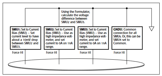
In the Formulator, the voltage difference between SMU2 and SMU3 is calculated and the resistance and sheet resistivity are derived from the voltage difference. The results appear in the Sheet tab of the ITM.
When making high resistance measurements, potential sources of error need to be considered in order to make optimal measurements. Use a probe head that has a level of insulation resistance between the probes that is sufficiently higher than the resistance of the material to be measured. This will help prevent errors due to leakage current through the probe head.Ensure that the measurement circuit is electrostatically shielded by enclosing the circuit in a metal shield. The shield is connected to the LO terminal of the 4200. The LO terminal is located on the GNDU or on the outside shell of the triax connectors. Use triax cables to produce a guarded measurement circuit. This will prevent errors due to leakage current and significantly reduce the test time. Finally, the Model 4200-PA preamp option is required to source very small currents (nanoamp and picoamp range) and to provide high input impedance (>1E16 ohms) to avoid loading errors when measuring the voltage difference.
The "LoR" ITM is only used for lower resistance materials and requires only one or two SMU instruments. In this case, the Force and Sense terminals of the SMU instruments are connected to the four-point probe as shown in Figure 20.
In the configuration shown in Figure 21, the Force HI terminal SMU1 sources the current through Probe 1. The voltage difference between Probes 2 and 3 is measured through the Sense terminals of the two SMU instruments.
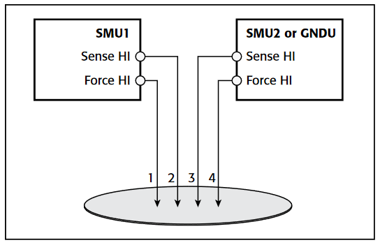
To compensate for thermoelectric offset voltages, two voltage measurements are made with currents of opposite polarity.The two measurements are combined and averaged to cancel the thermoelectric EMFs. The "LoR" ITM performs this offset correction automatically by sourcing the two current values in the List Sweep and then mathematically correcting for the offsets in the Formulator. The corrected resistance and sheet resistivity are displayed in the Sheet tab.
Measuring Resistivity with the van der Pauw Method
The van der Pauw (vdp) technique for measuring resistivity uses four isolated contacts on the boundary of a flat, arbitrarily shaped sample. The resistivity is derived from eight measurements made around the sample as shown in Figure 22.
Once all the voltage measurements have been taken, two values of resistivity, ρA and ρB, are derived as follows:
| ρA = | Π | fAts | (V2 + V4 - V1 - V3) |
| ln2 | 4I |
| ρB = | Π | fBts | (V6 + V8 - V5 - V7) |
| ln2 | 4I |
where:
ρA and ρB are volume resistivities in ohm-cm;
ts is the sample thickness in cm;
V1-V8 represent the voltages measured by the voltmeter;
I is the current through the sample in amperes;
fA and fB are geometrical factors based on sample symmetry, and are related to the two resistance ratios QA and QB as shown in the following equations (fA = fB = 1 for perfect symmetry).
QA and QB are calculated using the measured voltages as follows:
| QA = | V2 - V1 |
| V4 - V3 |
| QB = | V6 - V5 |
| V8 - V7 |
Also, Q and f are related as follows:
| Q - 1 | = | f | arc cosh ( | e0.693/f | ) |
| Q + 1 | 0.693 | 2 |
A plot of this function is shown in Figure 23. The value of "f" can be found from this plot once Q has been calculated.
Once ρA and ρB are known, the average resistivity (ρAVG) can be determined as follows:
| ρAVG = | ρA + ρB |
| 2 |
Using the vdp_resistivity subsite and vdp method ITMs
To automate the vdp resistivity measurements, the SolarCell project has a vdp-resistivity subsite with four ITMs: "I1_V23", "I2_V34", "I3_V41", and "I4_V12." A screenshot of the test is shown in Figure 24.
Each terminal of the sample is connected to the Force HI terminal of an SMU instrument, so a Model 4200-SCS with four SMU instruments is required. The four SMU instruments are configured differently in each of the four ITMs – one SMU instrument supplies the test current, two are configured as voltmeters, and one is set to common. This measurement setup is repeated around the sample, with each of the four SMU instruments serving a different function in each of the four ITMs. A diagram of the function of each SMU instrument in each ITM is shown in Figure 25.
Adjusting the Test Parameters
Before executing the test, some of the test parameters must be adjusted based on the sample to be tested. In particular, it's necessary to specify the source current, the settling time, and the thickness of the material.
Input Source Current: Before running the project, input the current source values based on the expected sample resistance.Adjust the current so that the voltage difference will not exceed approximately 25mV to keep the sample in thermal equilibrium.In each of the four ITMs, enter both polarities of the test current.The same magnitude must be used for each ITM.
Input the Settling Time: For high resistance samples, it will be necessary to determine the settling time of the measurements.This can be accomplished by creating an ITM that sources current into two terminals of the samples and measures the voltage drop on the adjacent two terminals. The settling time can be determined by taking multiple voltage readings and then graphing the voltage difference as a function of time.
This settling time test can be generated by copying and then modifying one of the existing vdp ITMs. Switch the source function from the sweep mode to the sampling mode. Then, in the Timing menu, take a few hundred or so readings with a delay time of one second. Make sure that the "Timestamp Enabled" box is checked. After the readings are done, plot the voltage difference vs. time on the graph. The settling time is determined by observing the graph and finding the time when the reading is within the desired percentage of the final value.
Input the Thickness of the Sample: Enter the thickness of the sample into the Calc sheet at the subsite level. Select the subsite vdp_resistivity. Go to the Subsite Data vdp-device tab. It contains the output values of the voltage differences and test current.From the Calc tab, the thickness can be adjusted. The default thickness is 1cm.
Input Correction Factor: The resistivity formula found in the Calc sheet at the subsite level also allows inputting a correction factor, if necessary. The resistivity is multiplied by this number, which may be based on the geometry or uniformity of the sample. By default, the correction factor is 1.
Running the Project
The van der Pauw resistivity measurements must be run at the subsite level. Make sure that all four checkboxes in front of the vdp ITMs ("I1_V23", "I2_V34", "I3_V41", and "I4_V12") are checked and then click on the subsite vdp_resistivity. Execute the project by using the subsite Run button (circular arrow). Each time the test is run, the subsite data is updated. The voltage differences from each of the four ITMS will appear in the Subsite Data vdp-device Sheet tab. The resistivity will appear in the Subsite Data Calc sheet as shown in Figure 26.
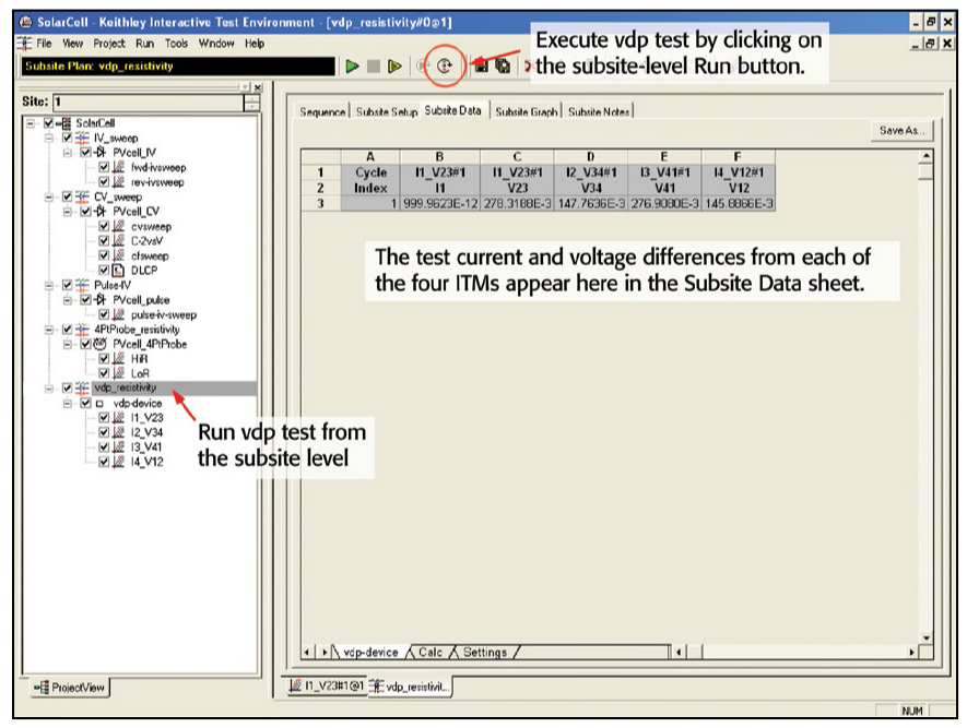
Hall Voltage Measurements
Hall effect measurements are important to semiconductor material characterization because the conductivity type, carrier density, and Hall mobility can be derived from the Hall voltage.With an applied magnetic field, the Hall voltage can be measured using the configuration shown in Figure 27.
With a positive magnetic field (B-), apply a current between Terminals 1 and 3 of the sample, and measure the voltage drop (V2–4+) between Terminals 2 and 4. Reverse the current and measure the voltage drop (V4–2+). Next, apply current between Terminals 2 and 4, and measure the voltage drop (V1–3+) between Terminals 1 and 3. Reverse the current and measure the voltage drop (V3–1+) again.
Reverse the magnetic field (B-) and repeat the procedure, measuring the four voltages: (V2–4–), (V4–2–), (V1–3–), and (V3–1–).Table 3 summarizes the Hall voltage measurements.
Table 3. Summary of Hall Voltage Measurements
| Voltage Designation | Magnetic Flux | Current Forced Between Terminals | Voltage Measured Between Terminals |
| V2–4+ | B+ | 1–3 | 2–4 |
| V4–2+ | B+ | 3–1 | 4–2 |
| V1–3+ | B+ | 2–4 | 1–3 |
| V3–1+ | B+ | 4–2 | 3–1 |
| V2–4– | B- | 1–3 | 2–4 |
| V4–2– | B- | 3–1 | 4–2 |
| V1–3– | B- | 2–4 | 1–3 |
| V3–1– | B- | 4–2 | 3–1 |
From the eight Hall voltage measurements, the average Hall coefficient can be calculated as follows:
| RHC = | t(V4-2+ - V2-4+ + V2-4- - V4-2-) |
| 4BI |
| RHD = | t(V3-1+ - V1-3+ + V1-3- - V3-1-) |
| 4BI |
where:
RHC and RHD are Hall coefficients in cm3/C;
t is the sample thickness in cm;
V represents the voltages measured in V;
I is the current through the sample in A;
B is the magnetic flux in Vs/cm2
Once RHC and RHD have been calculated, the average Hall coefficient (RHAVG) can be determined as follows:
| RHAVG = | RHC + RHD |
| 2 |
From the resistivity (ρAVG) and the Hall coefficient (RH), the Hall mobility (µH) can be calculated:
| µH = | RH |
| ρAVG |
Using the Model 4200-SCS to Measure the Hall Voltage
The SolarCell project does not include a specific test to measure the Hall voltage; however, four ITMs can be added to the subsite for determining the Hall coefficient and mobility. Given that the configuration for the Hall measurements is very similar to the van der Pauw resistivity measurements, the vdp ITMs can be copied and modified for making the Hall voltage measurements.The modifications involve changing the functions of the SMU instruments. Figure 28 illustrates how to configure the four SMU instruments in the ITMs to measure the Hall voltage. Use the Output Value checkboxes on the Definition tab to return the Hall voltages to the subsite-level Calc sheet.
User Test Modules (UTMs) must be added to control the magnet. For a GPIB-controlled electromagnet, users can write a program using KULT (the Keithley User Library Tool) to control the magnitude and polarity of the electromagnet. The code can be opened up in a UTM within the project. Information on writing code using KULT is provided in Section 8 of the Model 4200-SCS Reference Manual.
If a permanent magnet is used, UTMs can be employed to create a Project Prompt that will stop the test sequence in the project tree and instruct the user to change the polarity of the magnetic field applied to the sample. A Project Prompt is a dialog window that pauses the project test sequence and prompts the user to perform some action. See Section A of the Model 4200-SCS Reference Manual for a description of how to use Project Prompts.
Finally, the Hall coefficient and mobility can be derived in the subsite-level Calc sheet. These math functions can be added to the other equations for determining resistivity.
Conclusion
Measuring the electrical characteristics of a solar cell is critical for determining the device's output performance and efficiency.The Model 4200-SCS simplifies cell testing by automating the I-V, C-V, pulsed I-V, and resistivity measurements and provides graphics and analysis capability. For measurements of currents greater than 1A, Keithley offers Series 2400 and Series 2600B SourceMeter Instruments that can be used for solar cell testing.
Making Proper Electrical Connections to Ensure Semiconductor Device Measurement Integrity
Introduction
Poor-quality electrical connections to the device under test (DUT) can compromise the measurement integrity of even the most powerful and sophisticated semiconductor testing system.For high speed pulse measurements, interconnect quality typically determines maximum bandwidth; for low current measurements, it often affects measurement speed and accuracy.This application note discusses the problems created by poor connections. Although it specifically addresses MOSFET measurements, the techniques and results discussed also apply to many other devices.
VDS–IDS curves
The most straightforward way to assess a MOSFET's overall performance is to take VDS-IDS curves for a set of gate voltages because these curves define the operating regions of the device.Pulsed I-V characterization, wherein voltages and currents are applied for a very short time and at a limited duty cycle, is a common way to measure these curves. Pulsed I-V measurements can reduce test times and allow characterizing a device without exceeding its safe operating area or causing device self-heating and the associated parameter shifts.
Two pulsed I-V channels are typically used to measure these curves on a MOSFET, with one connected to the gate and the other to the drain. The ground of each channel is connected to the MOSFET source pin.
To construct the transistor curves, the gate channel first applies voltage to the gate, then the drain channel sweeps VDS through a range of values, measuring the resulting current at each point. Next, the gate channel applies a different voltage to the gate and the process repeats, constructing the next transistor curve in the set.
Modern pulse instruments can produce very short voltage pulses (100ns or less) with rise times as fast as 20ns, so wide bandwidth is critical to obtaining good measurements. For optimal performance, both pulse generator channels should be connected with coaxial cables matched to the generator’s 50Ω output impedance. However, it is impossible to maintain 50Ω impedance all the way to a device on a wafer in practice; at some point, the ground must be connected to one pin and the signal to another, breaking 50Ω characteristic impedance (Figure 1).Minimizing the length of these non-coaxial ground and signal connections is crucial.
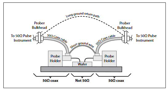
Figures 2a and 2b illustrate how inadequate grounding and coaxial cabling can produce erroneous data when characterizing a MOSFET using pulses with 20ns rise times, 20ns fall times, and a width of 200ns. Figure 2a shows data taken with 100W impedance triaxial cables and 1–2 ft. ground connections. Figure 2b shows data taken with 50Ω impedance coaxial cables and ground connections just a few inches long.The difference is striking: the data from an improperly cabled system are compressed (Figure 2a), measuring about half the level expected, while the data from the correctly cabled system (Figure 2b) match conventionally measured data.
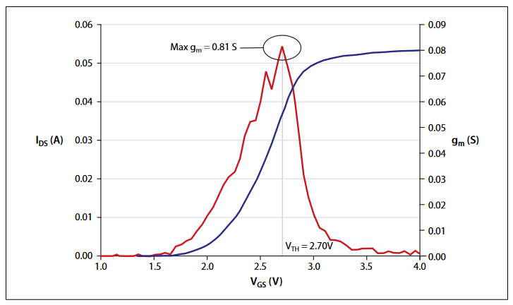
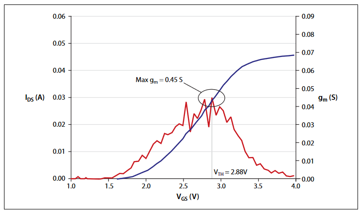
Maximum gm and VTH
Transconductance (gm) is a critical parameter widely used to determine the threshold voltage (VTH) of MOSFETs [1]. Pulsed I-V testing is ideal for this application because these parameters can be determined without violating safe operating area (SOA) limits or damaging the device
For a small signal analysis about a given gate and drain bias point, gm is defined as:
| gm = | ∂iDS |
| ∂VGS |
When measuring gm, the same connection scheme used to obtain the data in Figures 2A and 2B is used, but this time a DC voltage is applied to the drain while the gate voltage (VGS) is swept over the voltage range that transitions the device from off to on. Because the connections and pulsing speeds are the same, the earlier bandwidth discussion applies to gm and VTH testing as well.
Figures 3a and 3b show the results of another example of gm and VTH measurement, with the data shown in each taken with the same pulse rise and fall times, pulse widths, connections, and grounding. As Eq. 1 states, calculating gm requires computing the first derivative of the drain current with respect to the gate voltage.The blue curve is the drain current and the red curve is its calculated derivative.
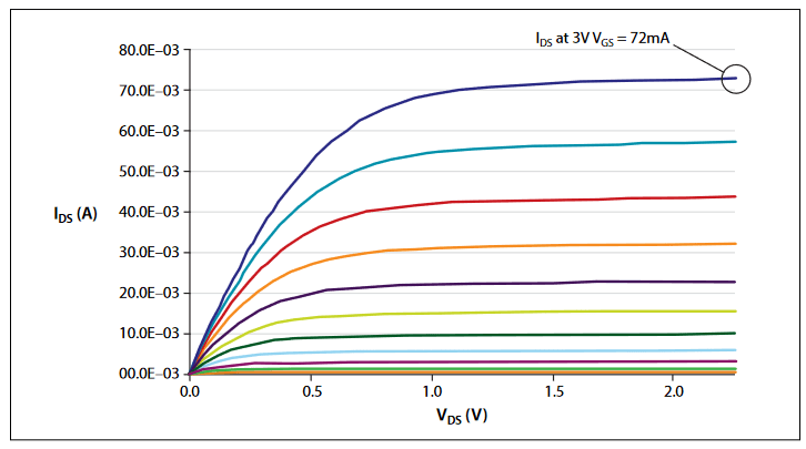
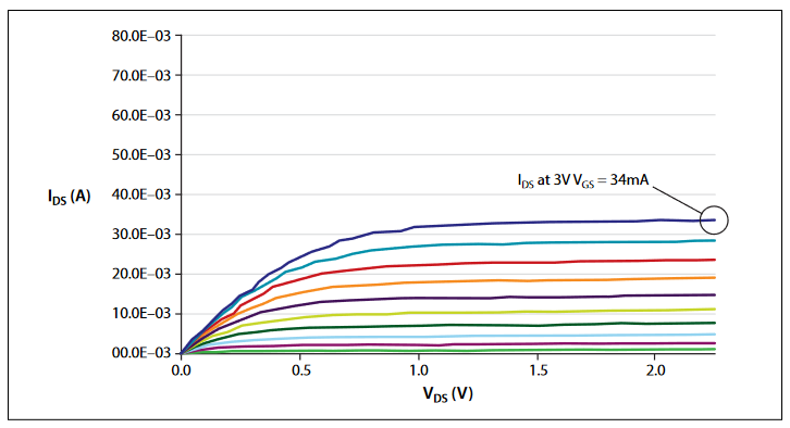
Just as with the VDS-IDS curves, the difference is significant. The results produced using the improperly cabled setup would mislead the user to think the DUT's gm is half its actual value and its VTH roughly 200mV higher than it actually is.
Capacitance-Voltage Testing
Capacitance-voltage (C-V) measurements are often used to characterize a MOSFET's gate oxide thickness, oxide defect density, doping profiles, etc. In this measurement, as the gate voltage varies, the capacitance of the gate to the drain and source changes. The Model 4210-CVU option allows Keithley's Model 4200-SCS Parameter Analyzer to make 1kHz–10MHz C-V measurements. It has four terminals wired to two device connections: CVU high and CVU low. In a standard C-V measurement, the source, bulk, and drain of a MOSFET are connected together and tied to CVU low; the gate is connected to CVU high. The Model 4210-CVU applies a DC bias and a small AC voltage to bias the transistor and simultaneously measure its capacitance, returning capacitance values for a wide range of bias voltages.
C-V measurements can be made at many frequencies (sometimes greater than 1MHz), depending on the parameters to be extracted. At higher frequencies, transmission line effects and cable length can impact measurement integrity significantly. For optimal C-V measurements, DUTs must be connected to the instrumentation using coaxial cables of the proper length and impedance level; for example, the Model 4210-CVU uses 1.5 meter, 100Ω cables.
Although using cables longer than those provided with the instrument will cause large changes in data at high frequencies, a feature known as cable length compensation can mitigate this problem.Using cables of different characteristic impedances, such as when coaxial cables are improperly adapted to triaxial cables, will also produce increased measurement error at high frequencies.
Off-State Leakage
Characterizing off-state leakage is critical to understanding quiescent power dissipation and transistor quality for small-scale parameter transistors. A source measure unit (SMU) instrument capable of measuring picoamp-level (1E–12A) currents is essential.
As with any low current measurement, properly guarded triaxial cables are essential. Using coaxial cables will produce erroneous results due to high cable capacitance (50Ω coaxial cables typically have 30pF of capacitance per foot). This capacitance must be charged with high currents before small currents flowing in the DUT can be measured, extending settling times substantially.
Triaxial cables alleviate this problem by providing a third conductor between the center pin and shell, called the guard, driven at the same potential as the center pin. The guard conductor drastically reduces the effective capacitance and reduces settling times. Never use poor-quality triaxial cables, which can introduce problematic dielectric absorption, triboelectric effects, or high noise.Unguarded cable segments should be minimized. For best performance, triaxial cables should be run as close to the DUT as possible.
Match the Cable to the Measurement
As these examples illustrate, matching cabling and grounding to the measurement type enhances measurement integrity. However, changing cables for each measurement type is so time-consuming many users simply tolerate the suboptimal results. Moreover, whenever cables are rearranged, users run the risk of reconnecting them improperly, thereby causing errors and demanding extra troubleshooting time. Worse still, these errors may go unnoticed for a long time.
One alternative is to use a remote switch capable of handling I-V, C-V and pulsed I-V signals, such as Keithley's Model 4225-RPM Remote Amplifier/Switch. When combined with a multimeasurement performance cable kit, such as Keithley's 4210-MMPC kit, it can often eliminate the need to recable between tests. This kit delivers the correct impedance and cable type, allowing low current, high speed pulse, and C-V measurements with no manipulator reconnection, eliminating the need to reprobe wafers.
Given the importance of characterizing semiconductor devices quickly and accurately, the value that the latest cable solutions can provide to device researchers is obvious.
Find more valuable resources at TEK.COM
Copyright © Tektronix. All rights reserved. Tektronix products are covered by U.S. and foreign patents, issu ed and pending. Information in this publication supersedes that in all previously published material. Specification and price change privileges reserved. TEKTRONIX and TEK are registered trademarks of Tektronix, Inc. All other trade names referenced are the service marks, trademarks or registered trademarks of their respective companies.
No.3250 1.21.14