How to Antenna Match with the Tektronix TTR500 in 5 Steps
Properly matching an antenna to a transceiver is one of the easiest ways to extend the signal range and battery life of a wireless product, such as those made for the internet of things. According to the inverse square law of radio waves, with only a 6dB improvement in path loss from improved matching, your device would transmit and receive at twice the range.
A spectrum analyzer with tracking generator can check an antenna match by looking at the voltage standing wave ratio (VSWR). However, the best tool to make the impedance measurements needed to effectively design a matching network is a vector network analyzer (VNA).
Unfortunately, many engineers tasked with integrating an antenna into a wireless product have had limited or no access to a VNA due to the historically high cost of these instruments, or they have not been trained on how to use one.
The Tektronix TTR500 vector network analyzer is a new affordable and easy- to- use option for performing antenna matching to improve the performance of wireless devices. In this post, we’ll walk you through a straight-forward process for antenna matching with the TTR500 VNA.
A similar process can be used for many other kinds of impedance matching needed to maximize power transfer between components in a system with high frequency signals or to check transmission line design or characteristic impedance.

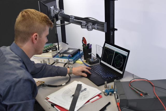
Figure 1. With the advent of portable USB-based VNAs, it's more affordable and convenient than ever to test and create your own antenna impedance matching network.
Why Impedance Matching is Important When Transmitting Power
Two primary factors that reduce the signal power transferred between a source and load, such as in a transceiver and antenna system, are signal reflections and power dissipation losses. Impedance mismatches between an antenna and transceiver cause signal reflections at the feed point of the antenna, which are either absorbed back by the source or dissipated by lossy transmission lines and components.
These reflections result in dramatically reduced signal range, dropped data packets, and wasted battery life. They can even damage the transceiver source if the reflected power is too high— – an extremely dangerous situation in high- power applications.
Maximum power transfer between a source and a load occurs when their resistances are the same, or for AC circuits, when their impedances are complex conjugates of one another. For example, some transceivers and antennas are specifically designed with impedances of 50 ohms (resistive) at their inputs (or outputs). In that case, they can be directly integrated and connected with 50- ohm transmission lines and achieve close to maximum power transfer.
In other cases, the input impedance of the antenna or load is not 50 ohms by design, or there is some imaginary part of the impedance (i.e. reactance) not accounted for that results in a mismatch. In this situation, a matching network is used to match the antenna, including its feed line, to the impedance of the source.

When it comes to antennas, although their datasheets or reference designs may say impedance is 50 ohms that may not be true for your environment or frequency of interest. At high enough frequencies, the input impedance of an antenna and connected feed line is highly dependent on the length of the feed line.
Additionally, any objects placed around an antenna, such as an enclosure or product packaging, will alter its radiation pattern, thus altering its input impedance. That’s why it’s important to use a VNA to measure the input impedance of the antenna (including its intended feed line) within the environment that will most closely resemble where it is intended to operate.
To combat circuit losses, in most cases, the matching network consists of one or more low-loss inductors and capacitors or transmission line stubs. These components are used in a network design chosen to meet the goals of matching, as well as any filtering and bandwidth (or multi-band) specifications as needed. Even an RF novice can correctly match an antenna using a vector network analyzer. The following five steps show you how.
The 5 Steps to Matching an Antenna to a Transceiver
Before we begin, it’s important to keep in mind that the impedance to be matched must be measured at the point where the matching network will be placed. As mentioned before, if there is transmission line (i.e. feed line) between the antenna port and the matching network location, it will affect the complex impedance value that must be matched with a matching network. This really only starts to become significant as the length of the feed line becomes greater than approximately 1/10th the wavelength of the highest frequency of interest.
Likewise, a VNA measures at the plane of calibration by default (i.e. without de-embedding or port extensions applied). So, any transmission line between the calibration plane and the matching network location must be accounted for. A port extension can be used to extend the calibration plane to the correct location if needed. Figure 1 illustrates these points.

Figure 2. The impedance measurement must be made at the point where the matching network will be placed. If additional transmission line length exists between the calibration plane and the intended matching network location, use a port extension to extend the calibration plane to the correct location.
Step 1 - Calibrate the VNA as close to the measurement plane as possible (i.e. the matching network location)
Getting the calibration plane dialed in correctly is the most crucial and difficult step in matching network design. A poor calibration can result in significantly different results. You don’t want to go through and design a matching network only to find out that you calibrated incorrectly. The compact arrangement and lack of compatible access points on most circuit boards and wireless modules makes this task a challenge. Typically, you have two options:
- Indirect: Calibrate with a commonly -available calibration kit, such as a 3.5mm cal kit compatible with SMA connectors, as close to the matching network as possible. You can then use a port extension to account for any adapters, transmission lines, or probes between the calibration plane and the matching network (see Step 2 below). One useful trick for getting the calibration plane close to the matching network location (if you can accomplish it) is to carefully solder a U.FL connector at the matching network location of your wireless module, calibrate the VNA with a 3.5mm cal kit, and use an SMA- to- U.FL adapter between the calibration plane and matching network location. A port extension can then be used to remove the adapter from the measurement.
- Direct: Create your own short, open, and load at the matching network location and perform an SOL calibration directly. This approach must be used very carefully, however, because it is difficult to create an ideal short, open, or load on a circuit board by soldering and de-soldering components. For example, a modestly oversized solder blob can add a significant amount of reactance to the measured circuit. However, for circuits at frequencies of 2 GHz and below, this shouldn’t be much of a problem because the wavelengths are relatively large.
Figure 2 illustrates these two approaches. The importance of a good calibration for getting an accurate impedance measurement cannot be overstated. If the calibration is off, the impedance measurement will be incorrect, and the match will not behave as expected when modifying the matching network. In that case the user will end up chasing the impedance around the 50- ohm point and waste time with multiple iterations.

Figure 3. Two options for calibrating and connecting the VNA.
Step 2 – If necessary, align the calibration plane with the measurement plane by using a port extension.
As shown in Figure 1 above, a transmission line between the VNA calibration plane and the matching network location will impact the measured impedance. This effect can be corrected reasonably well with a port extension. To understand how a port extension works, and how it affects the Smith chart display, let’s first review some Smith Chart basics.
The Smith Chart, shown in Figure 3, looks intimidating to the novice, but is easy to understand when you break it down. Begin with the polar reflection coefficient chart (Figure 4a below). As discussed earlier in this post, signal reflections, represented by the reflection coefficient, are related to the ratio of impedance at a mismatch.
Because we usually have a known reference impedance (Z0) of 50 ohms, the normalized load impedance ZL (the value normalized to 50 ohms) can be mapped onto the reflection coefficient chart. Note that impedance is a complex value consisting of real and imaginary parts (i.e., Z = R + jX). When we map ZL to the reflection coefficient chart, some useful patterns emerge: lines of constant resistance, R (Figure 4b) and lines of constant reactance, X (Figure 4c).

Figure 4. Smith Chart (Impedance)

Figure 5a. Polar reflection coefficient chart with dotted lines of constant reflection coefficient magnitude / constant VSWR.

Figure 5b. Smith Chart with lines of constant resistance (R).

Figure 5c. Smith Chart with lines of constant reactance (X).
Finally, getting back to port extensions, changing the length of a transmission line between the measurement point and the impedance mismatch does not change the magnitude of reflection; however, it does change the measured phase. This results in a rotation on the Smith Chart around the 50- ohm center point along a line of constant reflection coefficient magnitude / constant VSWR (Figure 5a).
An increase in transmission line length will result in a clockwise rotation along the Smith Chart. If this phase difference is not accounted for, the impedance value measured by the VNA will be different than the value at the matching network location, and the wrong matching network values will be chosen to match the antenna. The phase correction can be made using a VNA by applying a port extension.
Figures 6a and 6b illustrate the rotation of a trace on a Smith Chart using a port extension with VectorVu-PC software and the TTR500 VNA. The value referred to as delay length in the port extension dialogue box is the physical length between the calibration plane and the desired measurement plane. An easy way to set the port extension correctly is to place an open or short circuit at the desired measurement plane (the matching network location) and incrementally adjust the delay length or delay time until the S11 trace moves to the corresponding position on the right (open) or left (short) side of the Smith Chart (Figure 6b below).
Adding a positive value results in a counterclockwise rotation. A negative value results in a clockwise rotation. While in most cases, removing the DUT (i.e. matching network) will conveniently leave a suitable open at the desired reference plane, an open is susceptible to fringing capacitance and other parasitics at higher frequencies that make it less than ideal. Therefore, it may be best to use a short if your center frequency is above a gigahertz or two.
Now you’re ready to measure the unmatched impedance at the matching network location. You can also check out this link for a video tutorial of applying a port extension with the TTR500.

Figure 6a. Smith chart with no port extension applied.

Figure 6b. Smith chart with a 4.9 cm port extension.
Step 3 – Measure the unmatched impedance at the frequency of interest.
Using a VNA, measure S11 and view the trace on a Smith Chart display. To get a clearer, more relevant trace, configure the VNA to sweep only over the frequency span covering the band(s) of interest (see Figure 6 below).
Depending on your approach in Step 4 below, save the trace to a .s1p file or record the R+jX impedance value at the frequency of interest. Setting a marker at the mid-band point(s) will help you identify how the trace needs to move on the Smith Chart to get to the 50-ohm match point. Or, if you only need the single impedance value in the middle of a band, you can configure a zero-span trace at the mid-band frequency to easily distinguish the impedance at that frequency point.

Figure 7. Example of an unmatched antenna impedance measurement (ZL = 79.1 – j69.87 Ω). Either save the full .s1p file or record the center frequency impedance value to calculate the matching network.
Step 4 - Determine the matching network component values and integrate the components.
These days, few people calculate the matching network component values by hand (although I applaud those who still do). There are a variety of matching network circuit simulators available, ranging from free downloadable tools to professional tools like Optenni Lab that provide powerful features to optimize a matching network based on multiple performance needs and design constraints.
A PC-based VNA like the TTR500 saves you time by making it easy to save s-parameter files from the VNA (containing the impedance measurement information) and import them into the circuit simulator.
Although the Smith Chart is rarely used these days to calculate matching component values, it is a very useful tool for visualizing how the choice of components will move the impedance from the unmatched value along the chart lines to the 50-ohm center point. For an excellent learning site on Smith Charts and matching, check out www.antenna-theory.com.
Step 5 – Confirm the matched impedance, and adjust if needed.
Once the matching network is integrated, re-measure the impedance in the same way as in Steps 2 and 3. With a little luck, the trace will be centered and the antenna will now be matched to 50 ohms.! If the impedance did not shift on the Smith Chart consistent with what was predicted based on the matching circuit design, the most likely culprit is that the measured impedance was incorrect due to an inaccurate calibration (or incorrectly-applied port extension).
In that case, try re-performing the calibration or establishing the calibration with a different approach. Using a cal kit may be a preferred option instead of trying to create a SOL on the PCB board). You may also have difficulty establishing a clean calibration as a result of the sensitivities of impedance measurement to board and test setup parasitics. In that case, you can try to iterate the matching network component values through trial -and- error until the antenna match is acceptably close to 50 ohms.


Figure 8. Example: fully matched (yellow) vs. unmatched antenna (purple). The unmatched antenna is only achieving 4 to 5 dB return loss, resulting in as much as 30-40% reflected power. The fully matched antenna is achieving greater than 40 dB return loss, indicating a reflected power of less than 1%.
With those five steps and the TTR500 vector network analyzer from Tektronix, anyone can improve their wireless device’s performance without breaking the bank. You can also check out the TTR500 in action in this antenna matching tutorial video as well as many other TTR500 video tutorials.
In the video, thanks to simple antenna matching, we were able to improve path loss between two antennas by as much as 6 dB, thereby doubling their potential transmit range. You can also learn more about the TTR500 by visiting Tek.com, where you can also find options to sign up for a quote or free demo.